VIDYA VIJAY, CyberOptics
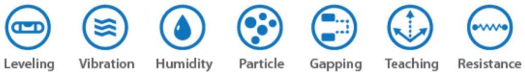
Setup and maintenance operations for semiconductor manufacturing tools can be tedious, time-consuming, and expensive, incurring both direct costs for personnel and resources and indirect costs for lost tool time during extended commissioning of new tools and requalification of repaired or serviced tools. Wafer-like (and reticle-like) sensors (WaferSense® from CyberOptics) provide fast, easy access for measurements inside the process chamber. Over the years, sensors have been developed for many routine measurement tasks, including leveling, vibration, humidity, particles, gapping, teaching, and resistance. Two new teaching sensors provide enhanced capabilities for fine-tuning the movement of position-critical internal components like robot end-effectors and wafer carriers. In some applications, these sensors can reduce the time required to perform setup and maintenance operations by a factor of ten or more.
There are a number of critical in-chamber measurement operations that may impose inordinately large costs when they are required. They may be occasional, associated with tool setup or major maintenance and repair, or they may be routine, such as monitoring for particles or measuring gaps to ensure tool matching. They are often simple in concept but made difficult by poor access and limited space inside a process chamber. Their measurement cycles are often extended by the stringent requirements of the process environment for cleanliness, demanding lengthy cleaning and requalification cycles when anything foreign has entered the chamber.
Consider something as simple as aligning a wafer chuck or a robot arm. It can be done with hand tools, perhaps a ruler and a level, but the challenge comes in gaining access to components inside the process chamber. The more the chamber is opened to allow access the greater the risk of contamination from the tools, the operator, or the ambient fab environment, and the more time it takes to return the tool to service.
These are the challenges that led to the development of the first wafer-like sensors – if you want to see what a wafer sees inside the chamber, wouldn’t it be good to look like a wafer. The same logic led also to the development of sensors designed to mimic reticles. Sensors are now available for leveling, vibration, humidity, gapping, teaching, and resistance (FIGURE 1). All sensors are battery powered and communicate with the host by radio (Bluetooth).

Wafer-like and reticle-like sensors can:
- Save time and reduce cost
- Improve yields and increase tool uptime
- Increase throughput
- Reduce resource needs
- Speed equipment set-up, maintenance cycles, troubleshooting, qualification, and release to production
- Speed tool optimization, stabilization, and standardization
- Streamline fab processes
- Establish repeatable and verifiable standards
Click here to read the full article in Semiconductor Digest magazine.