CHRIS MACK, Co-Founder and Chief Technology Officer, Fractilia
There’s a new class of yield killers in semiconductor fabs and chipmakers are spending hundreds of millions of dollars to deal with them.
They’re called stochastics, and they are random and non-repeating patterning errors with causes that are very different from conventional non-repeating defects.
Stochastics have been around for years, but until recently they were much smaller than the feature sizes of leading-edge chips, so the semiconductor industry has largely been able to ignore them. However, while stochastic effects have largely remained the same size over the years, the feature sizes themselves have continued to shrink, to the point where stochastics have now become a much larger percentage of the fab error budget (see FIGURE 1 for an example).

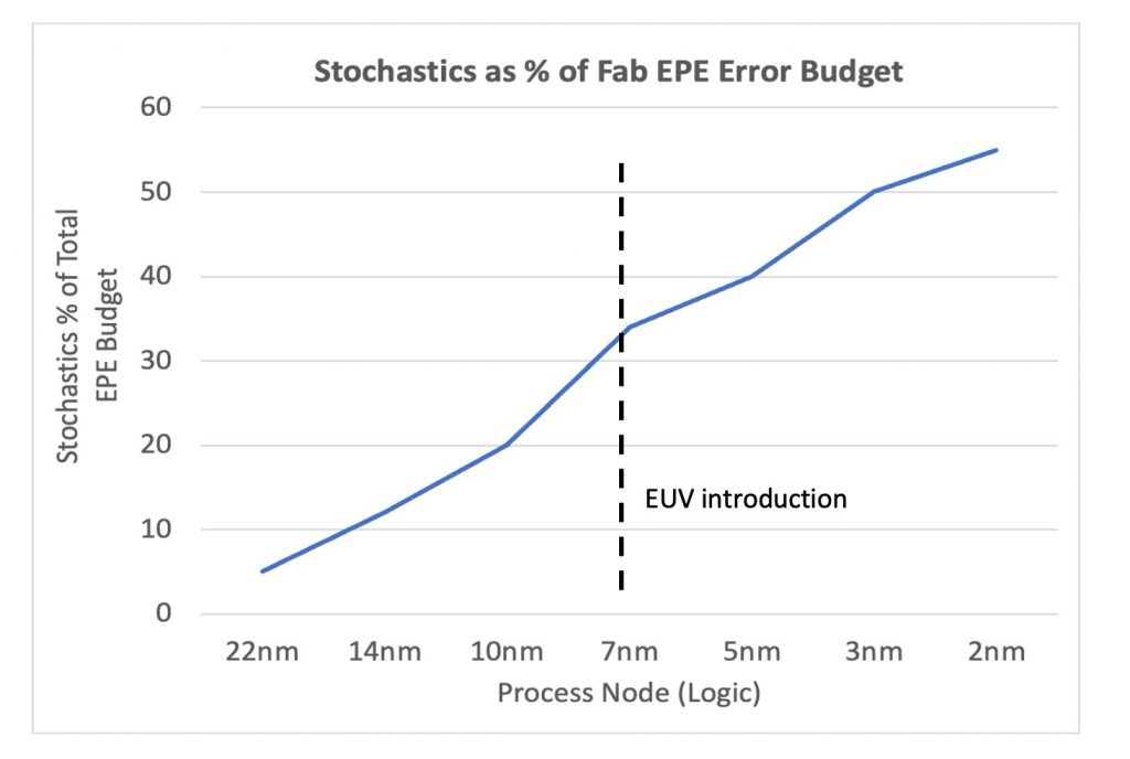
Stochastics have become an even worse problem with the adoption of EUV lithography, where on top of feature size scaling, photon shot noise has significantly added to stochastic variability. Going forward, stochastics will represent more than half of an EUV fab’s edge placement error (EPE) budget, making them a major problem for any device manufacturer doing EUV – a problem that is only getting worse. There are four major categories of stochastics: EPE, local critical dimension uniformity (LCDU), line edge roughness/line width roughness, and stochastic defects. All of these stochastic effects impact device performance, reliability, and yield. And, with the introduction of EUV and continued shrinking to smaller nodes, stochastics have become the predominant source of patterning variation in the semiconductor industry.