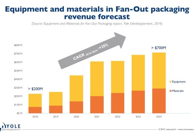
Key players from different business models are fueling new growth.
Update: TSMC’s 5nm CMOS Technology Platform
At the International Electron Devices Meeting (IEDM) in San Francisco December 7-11, Geoffrey Yeap presented the talk “5nm CMOS Production Technology Platform Featuring Full-Fledged EUV and High-Mobility Channel FinFETs with Densest 0.021µm2 SRAM Cells for Mobile SoC and High-Performance Computing Applications”. Contributing Editor Dick James provides an update on his original pre-IEDM blog.
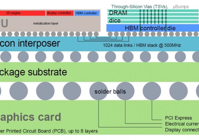
The History and Future of DRAM Architecture in Different Application Domains: An Analysis
Common trends and bottlenecks in DRAM architecture are identified.
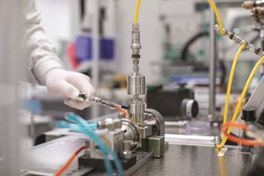
Swagelok Introduces New ALD20 UHP Valve
The ALD20’s patent-pending design maximizes production process efficiency and deposition consistency by providing flow coefficients two to three times what can be achieved using today’s standard ALD valve technology.
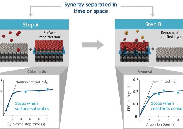
Nanoscale Features through Atomic Layer Processing
Atomic layer etching and deposition processes offer atomic scale control through the use of self-limiting reactions.
SLO Cables for Vacuum Application
A new solution that combines ‘super’ low outgassing (SLO) cables with flexibility and integration of multiple cables is designed for applications with moving parts in vacuum chamber environments ranging from motors to encoders.
2019 Global Silicon Shipments Dip From 2018 Record High But Revenue Remained Stable Above $11 Billion
Worldwide silicon wafer area shipments in 2019 declined 7 percent from the 2018 record high while revenue remained above the $11 billion mark despite a global silicon revenue slip of 2 percent over the same period, the SEMI Silicon Manufacturers Group (SMG) reported in its year-end analysis of the silicon wafer industry. Silicon wafer area shipments in 2019 totaled 11,810 million square inches (MSI), while the industry logged shipments of 12,732 million square inches in 2018. Revenues in 2019 totaled $11.15 billion, edging down from the $11.38 billion posted in 2018.
CEA-Leti Develops Tiny Photoacoustic-Spectroscopy System For Detecting Chemicals & Gases
Leti, an institute of CEA-Tech, has developed a photoacoustic spectroscopy technology for monitoring dangerous chemical emissions and traces of gas that could reduce the cost and the size these systems by a factor of 10 or more compared to existing tools. To be presented in an invited paper at Photonics West 2020 titled “Micro PA detector: pushing the limits of mid-IR photoacoustic spectroscopy integrated on silicon”, the detector also provides high immunity to external noise and high sensitivity and selectivity.
ZEISS Accelerates Semiconductor Package Failure Analysis by Orders of Magnitude with Crossbeam Laser FIB-SEM
ZEISS today introduced the ZEISS Crossbeam Laser — a new family of site-specific focused ion beam scanning electron microscope (FIB-SEM) solutions that accelerate package failure analysis and process optimization for advanced semiconductor packages. Integrating a femtosecond laser for speed, a gallium ion (Ga+) beam for accuracy, and SEM for nanoscale-resolution imaging, the ZEISS Crossbeam Laser family provides package engineers and failure analysts with the fastest cross-section solution at the highest imaging performance, while providing minimal sample damage.
SEMI Postpones SEMICON China, Suspends SEMICON Korea in Response to Coronavirus Outbreak
In accordance with government guidelines and to protect the health and safety of exhibitors and guests, SEMI announced Tuesday the postponement of SEMICON/FPD China 2020 and related events originally scheduled for March 18-20, 2020. SEMI China is actively working on a contingency plan for rescheduling of the event and will keep you informed as soon as a confirmed plan is in place.