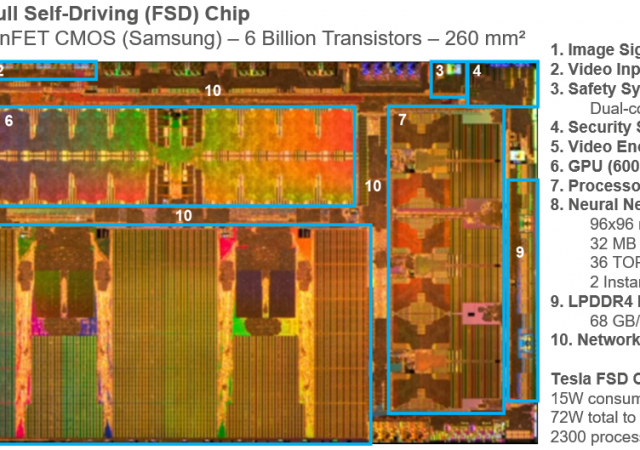
Tesla’s autopilot chip executes 72-trillion additions and multiplications per second: It better get the math right
Development of Highly Sensitive Diode, Converts Microwaves to Electricity
The Japan Science and Technology Agency (JST), Fujitsu Limited, and the Tokyo Metropolitan University announced that they developed a highly sensitive rectifying element in the form of a nanowire backward diode, which can convert low-power microwaves into electricity. Through JST’s Strategic Basic Research Programs, the technology was developed by researchers led by Kenichi Kawaguchi of Fujitsu Limited and Professor Michihiko Suhara of the Tokyo Metropolitan University.
Achronix Joins TSMC IP Alliance Program
Achronix Semiconductor Corporation, a provider in FPGA-based hardware accelerator devices and high-performance eFPGA IP, has joined the TSMC IP Alliance Program, a key component of TSMC Open Innovation Platform® (OIP). Achronix’s award-winning Speedcore eFPGA IP is optimized for high-end and high-performance applications. Speedcore eFPGA IP is available today on TSMC 16nm FinFET Plus (16FF+) and N7 process technologies, and it will be soon available on TSMC 12nm FinFET Compact Technology (12FFC).
Samsung Introduces Industry’s First 0.7μm-pixel Mobile Image Sensor
Samsung Electronics Co., Ltd. today introduced the industry’s first 0.7-micrometer (μm)-pixel image sensor, the 43.7-megapixel (Mp) Samsung ISOCELL Slim GH1. Thanks to advanced ISOELL Plus technology, the new ultra-high-resolution GH1 image sensor embraces 43.7-million 0.7μm-sized pixels in a super-small package, providing the optimum solution for slim full-display devices.
UMC Receives Final Approval for 100% Acquisition of Mie Fujitsu Semiconductor
United Microelectronics Corporation (NYSE: UMC; TWSE: 2303) (“UMC”), a global semiconductor foundry, today announced that the company has satisfied all closing conditions, including final approval from all relevant government agencies, for the full acquisition of Mie Fujitsu Semiconductor Limited (MIFS), the former 300mm wafer foundry joint venture between UMC and Fujitsu Semiconductor Limited (FSL). The completion of the acquisition is scheduled for October 1, 2019.
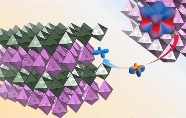
Bottom-Up Synthesis of Crystalline 2D Polymers
Scientists at the Center for Advancing Electronics Dresden (cfaed) at TU Dresden have succeeded in synthesizing sheet-like 2D polymers by a bottom-up process for the first time. A novel synthetic reaction route was developed for this purpose. The 2D polymers consist of only a few single atomic layers and, due to their very special properties, are a promising material for use in electronic components and systems of a new generation. The research result is a collaborative work of several groups at TU Dresden and Ulm University and was published this week in two related articles in the scientific journals “Nature Chemistry” and “Nature Communications”.
Iridium ‘Loses Its Identity’ When Interfaced With Nickel
Iridium “loses its identity” and its electrons act oddly in an ultra-thin film when interfaced with nickel-based layers, which have an unexpectedly strong impact on iridium ions, according to Rutgers University-New Brunswick physicist Jak Chakhalian, senior author of a Rutgers-led study in the journal Proceedings of the National Academy of Sciences.
Intel Updates Advanced Packaging Technologies at SEMICON West Part 3
The SEMICON West workshop was unusual in that all the presenters were from Intel’s Assembly Test Technology Development (ATTD) group, and the session kicked off with a review of ATTD by Corporate VP Babak Sabi. The scope of their activities ranges from wafer sort, die preparation, and identifying known good die, through assembly, test, die finish, and board development, and also substrates, tooling, and other assembly materials; so pretty well the whole spectrum. They have quite the complex in Chandler (Arizona), as well as other facilities in Oregon and Malaysia.
Revolutionizing Wafer Testing to Bring New Technologies to Market
Nearly every new technology breakthrough in the semiconductor industry targets high volume manufacturing and comes with its unique specificities. This results in challenges for engineers to manufacture and test new integrated circuits (ICs) on the wafer.
MagnaChip Targets Fast-Growing e-Bike Market with High-Performance MOSFET
MagnaChip Semiconductor Corporation, a designer and manufacturer of analog and mixed-signal semiconductor products, announced today the release of a 100V Mid-Voltage MOSFET with a new thermal package designed for the fast-growing e-Bike market. This MOSFET with M2PAK-7P is suitable to meet the particular requirements of electric bike (e-Bike) systems.