BOB CONNER, VP of Business Development at X-Celeprint
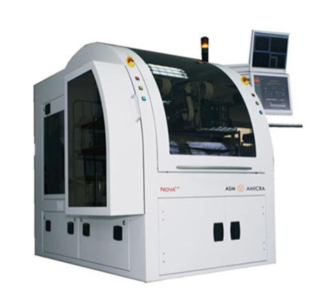
Dr. JOHANN WEINHÄNDLER, Managing Director at ASM AMICRA
Expanding heterogeneous integration (HI) from high end applications to high volume, cost sensitive applications will require significant reduction in manufacturing costs. One promising cost reduction approach is to employ large area panels and processing technologies from the printed circuit board, flat panel display, and solar panel industries rather than 300mm wafers for HI. Analog ICs are an attractive market-driver for panel-level HI, because the market is sufficiently large ($68 billion in 2021 [1]). Tightly integrating separately manufactured components increases the performance of power management, wireless communications, and other analog ICs by significantly reducing inductive and capacitive parasitics.
Analog ICs have different HI requirements than digital “compute” applications, which heterogeneously integrate processor, accelerator, high bandwidth memory, and other die in a system-in-package (SiP). Whereas compute applications require large body package sizes and high I/O density with <1/1 micron line/space requirements, analog ICs require small footprints and low I/O density. Therefore, >10/10 micron line/space is sufficient. HI analog ICs, such as power and RF transistors, require high current density (A/mm2) and thermal density (W/mm2).
Micro-transfer printing (MTP), a massively parallel pick-and-place process developed by X-Celeprint, may be used to produce HI analog ICs comprised of large arrays of ultra-thin (2-20 micron) separately manufactured components, called x-chips, interconnected using redistribution layer (RDL) technology. The MTP process consists of the following steps:
Source Wafer Fabrication: Separately manufactured x-chips, made using the optimal process node and technology for each function, are fabricated on one or more source wafers. A sacrificial layer is formed underneath the x-chips using different techniques depending upon the source wafer technology. A tether/anchor system suspends the x-chips aloft after the source wafer is anisotropically etched to remove the sacrificial layer everywhere but underneath the anchor. The x-chips are tightly packed on the source wafer, reducing cost via high wafer utilization.
MTP Stamp Fabrication: MTP stamps are made with a low-cost, re-usable mold. Each stamp consists of an array of soft posts composed of a compliant elastomer material, polydimethylsiloxane (PDMS), on a stiff glass substrate. The stamp is stiff in the x-y dimensions, providing high placement accuracy, and is compliant in the z-dimension, accommodating non-planar and rough x-chips and panels. The stamp’s posts adhere to the x-chips via van der Waals forces. The stamp’s viscoelastic behavior uses fast separation speed during pick-up to break the tethers and remove the x-chips, and slow separation speed to place the x-chips on the panel. The pattern and spacing of the small posts on the MTP stamp are customized for selective pick-and-place to provide either tightly or loosely packed x-chip arrays on the panel.
Massively Parallel Pick-and-Place: ASM Amicra’s Nova+ MTP ultra-high precision, high throughput, fully automatic ISO clean room class 10 pick-and-place system (FIGURE 1) uses an MTP stamp (up to a 50x50mm) to transfer x-chips from one or more source wafers (up to 300mm) to the panel (up to 450x450mm) [2]. Placement accuracy is plus-or-minus 1.5-microns at three sigma with a 40-second cycle time. A “step and repeat” process populates a 450x450mm panel with x-chips in less than an hour. The stamp readily handles x-chips at the wafer’s edge, providing high source wafer utilization which reduces cost. The x-chips may be transferred from multiple source wafers to different locations within the same die on the panel to tightly integrate separately manufactured components.

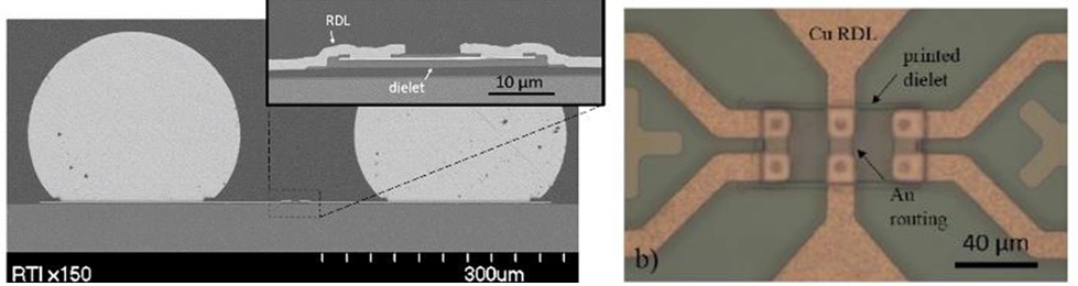
RDL Interconnects: Since the x-chips are ultra-thin, one or more RDL layers can readily interconnect the x-chips, reducing path lengths and parasitics. Since MTP inherently provides fan-out (FIGURE 2) and through x-chip vias (the gaps between the x-chips used for etchants to release the sacrificial layer), it eliminates many materials and processes used in traditional fanout, such as reconstituted dies’ epoxy molding compounds, and challenges, such as die shift, since a thin adhesive layer on the panel holds the x-chips in place prior to RDL.

Read the full article in the August/September issue of Semiconductor Digest.