PETER GILLESPIE, VP & GM, Semiconductor Products, Advanced Energy Industries, Inc., (AE) Milpitas, CA;
DAN CARTER, Member of Technical Staff II, AE, Fort Collins, CO;
DENIS SHAW, PhD, VP Semiconductor Integrated Solutions, AE, Fort Collins CO;
ISABEL YANG, PhD, Chief Technology Officer, AE, Denver, CO
This is the third article in a series highlighting the importance and transformation of process power in semiconductor manufacturing applications. The first article, “Process Power Steps Out from the Shadows,” uncovered the high-growth $1.2B process power market and how it has become a critical enabler for etch, deposition, and other processes such as ion implantation and e-beam inspection.
The second article, “Process Power: The New Lithography,” dove deep into how RF power delivery systems have innovated and been evolved as they were tapped to enable etch and deposition processes to “draw-in” device patterns between photolithography processing steps, especially in 3D memory devices and complex logic features. This underscored how process power has changed from formerly being viewed as a simple “dumb black box” to now being seen as the “new lithography.” The second article also revealed how RF generators and matching networks have become complex, highly synchronized systems with sophisticated controls and system-level power combinations including multi-frequency feeds, pulsing and micro-second response times.
This final article looks at the future of semiconductor manufacturing processing requirements and the new approaches that enable process applications at advanced technology nodes. It is clear that processes will require even faster speeds of response, additional control knobs, more direct ion energy distribution discrimination, the ability to transform available power data into actionable information, and, as always, remain under relentless pressure for lowest cost and smallest size. Solutions to these challenges will be discussed including integrated RF and tuning networks, solid-state tuning networks, non-sinusoidal bias for tailored ion energy distribution, and predictive power delivery.
A bigger process power toolbox
The semiconductor manufacturing industry has consistently moved forward via both incremental progress (improving and evolving what has worked) and innovation (new capabilities and disruptive approaches). Manufacturing devices near and below 7 nm technology nodes brings new challenges that require novel process power innovations and, at the very least, a bigger toolbox of process power capabilities.
The need for greater process power agility and response speed is driven by many shorter process steps, within longer process recipes. The power level is critical during every microsecond in deposition to control film stress and in etch to manage the plasma through frequent, abrupt, and profound changes in flow, pressure, power and chemistry that wildly swing plasma impedance. This requires repeatable and reproducible power delivery.
As 3D device stack layer counts have gone from tens to hundreds and features get ever deeper and narrower, the end of the horizon for simply increasing RF power is coming into focus. Very high RF bias powers (increasing to 50 kW and beyond to potentially as high as 100 kW) are likely not sustainable for clean power delivery and the tight control required; and additionally, the potential for damage and premature chamber wear is significant. Aside from these risks, the power required for a six or ten chamber system with 100 kW of RF power on each chamber raises the stakes not just in complexity, but also for bulk power distribution, platform costs, and even environmental concerns for both system and fab. This is an example where innovation is required vs. incremental scaling.
Significant and emerging enablers in the process power toolbox are precision measurement and control of power, and with these, the acquisition and use of power control parameter information. As process power has become more complex, a rich array of available information has been amassed from onboard power metrology, control loops, and tuning network states. This information, parsed through the domain of power expertise, provides insight that can be leveraged to learn, optimize, and predict power parameters relevant to the process performance itself. This adds another whole dimension to the process power toolbox.
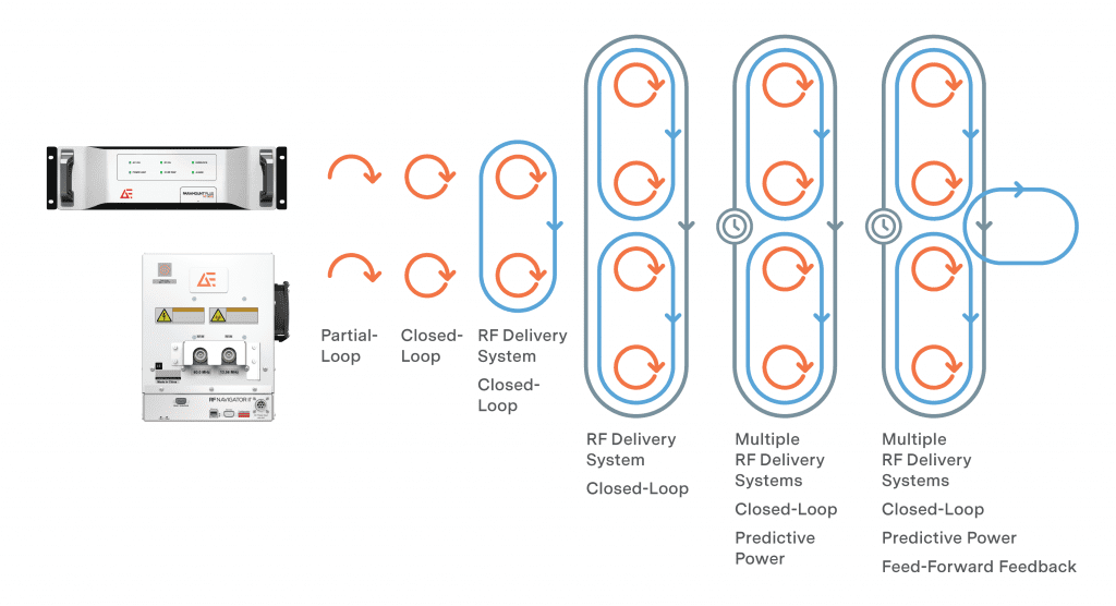
FIGURE 1 illustrates the evolution of process power control. Starting with simple command-and-response operation and open loop controls, such as forward power regulation in generators and manually tuned matches, the state of the art moved to closed loops using delivered power regulation and highly accurate auto-tuning match networks. Connecting loops to synchronize process power delivery at both source and bias enables pulsing and complex plasma control through sometimes only marginally stable plasma transitions. Predictive power machine learning can be added at the product, system, or multi-system level. Ultimately, there will be further linkage between process power information and broader system parameters for feed-forward and feedback.


Beyond process power capability and the use of control loops and predictive information, the increased cost and size of incremental solutions will also become showstoppers without implementing different approaches. Put together, these are reasons to look beyond the incremental and reach into a bigger process power toolbox that is described in this article.
Fast-and-small drives value of integration
Plasma-based deposition process applications such as Plasma Enhanced Chemical Vapor Deposition (PECVD) and Plasma Enhanced Atomic Layer Deposition (PEALD) process applications present unique challenges for RF process power delivery systems. Deposition applications, especially PEALD, are trending toward very short deposition steps with durations of one second or less. In addition, semiconductor manufacturing equipment (tools) used for these applications are often designed to process multiple wafers simultaneously while sharing a common vacuum (sub-atmospheric) management system.
These complex tools are tightly packed with pumps, valves, and other Critical Subsystems (CSubs) and hardware, limiting the available space for RF power systems. Deposition tools are also under arguably the tightest cost pressures in the plasma Wafer Fabrication Equipment (WFE) segment, and cost has been an ongoing motivation for novel approaches wherever possible to reduce overall system expense.
By their nature, deposition plasmas tend to utilize a more stable and predictable plasma impedance range compared to etch applications. The highly cyclical character of these PECVD and PEALD processes, combined with an understanding of their impedance behavior, sets up both the need for, and opportunities to, optimize power delivery for performance, longevity, and cost effectiveness. For these applications, the unique physical integration of power generation and highly responsive impedance matching has increasingly proven to be very effective, achieving multiple benefits in these demanding and cost sensitive process tools.
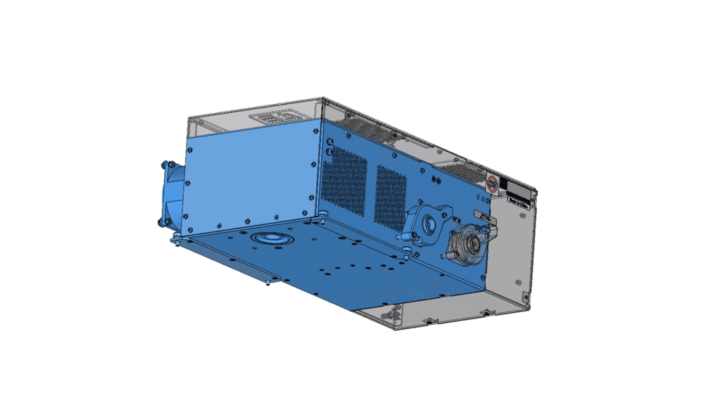
FIGURE 2 shows an example of an integrated RF power delivery solution for PECVD. In this case, an electrically switchable solid-state capacitor array is physically integrated with the RF power amplifier to produce a small form-factor power delivery system in a single enclosure. The overall package size is nearly equal to a traditional RF power generator, but this design includes the matching network within the common enclosure. (Recall from the second article in this series, RF generators and matching networks are most commonly separate “boxes” connected by a power cable.) The integrated package permits mounting directly to the wafer pedestal connection and further saves space that would otherwise be necessary with traditional non-integrated, rack-mounted power supplies.

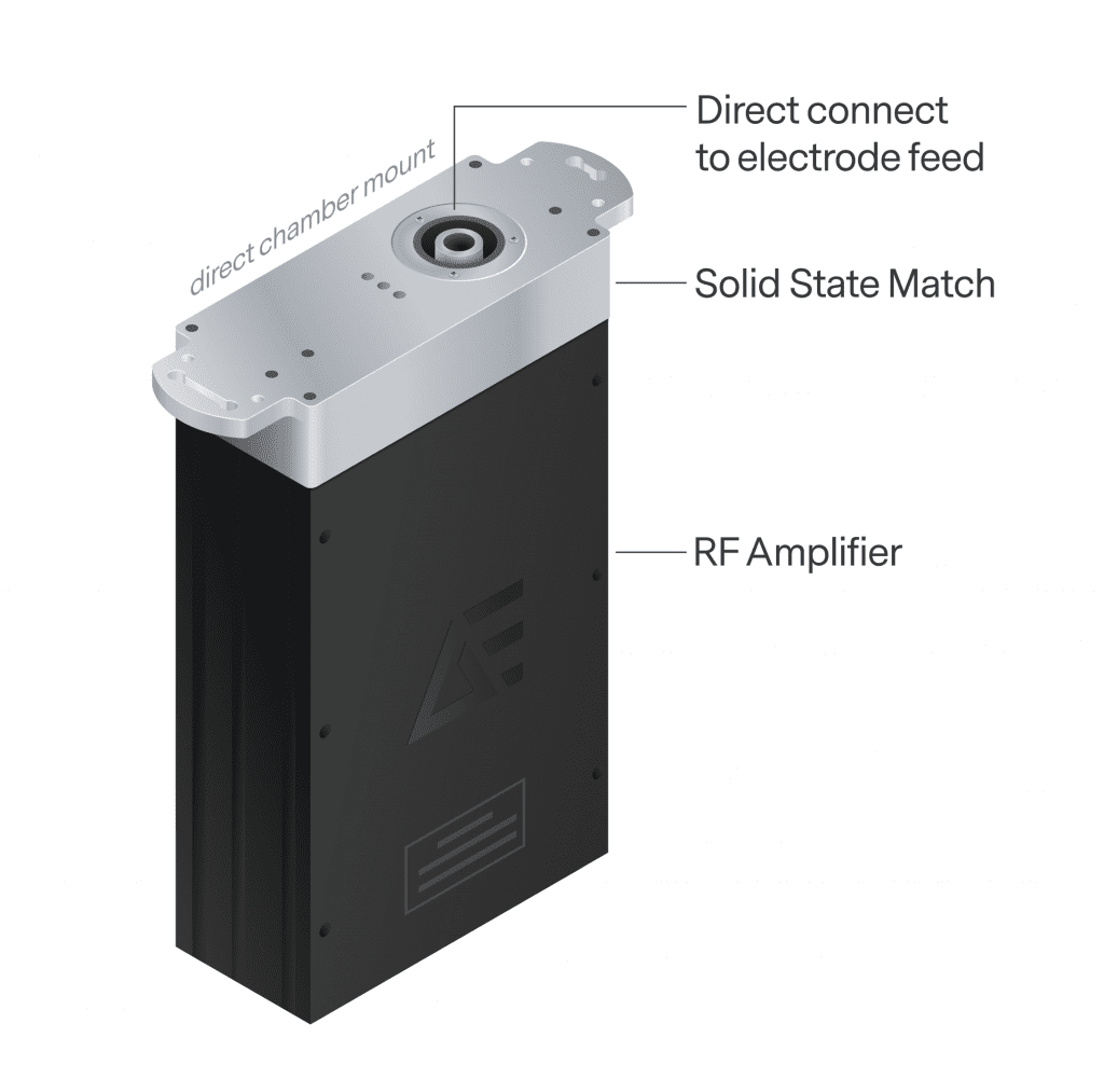
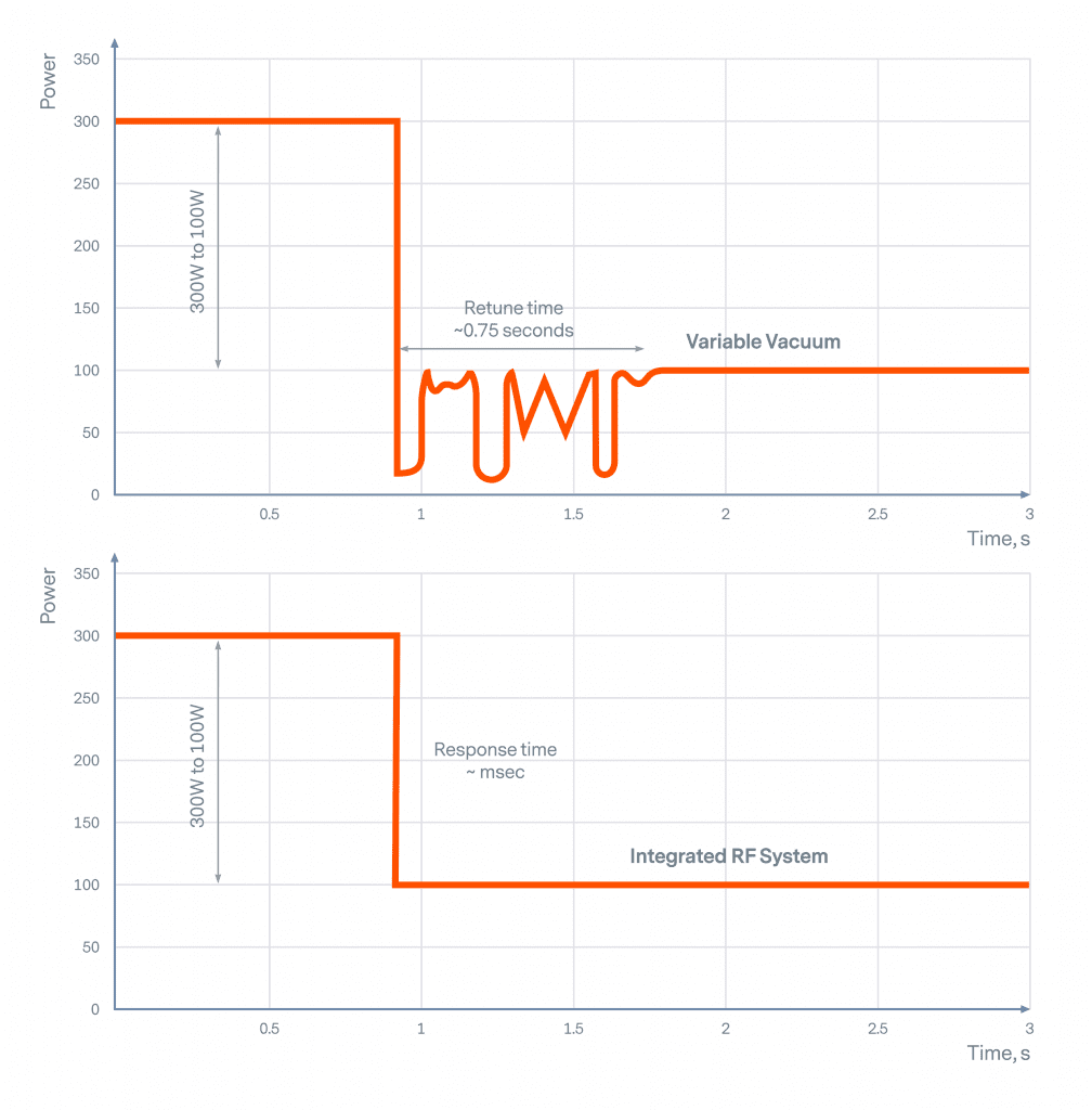
In addition to space savings, mechanically driven vacuum capacitors are replaced in the integrated matching network with solid state components that are more reliable and repeatable, both especially valuable attributes in these high-cycle, repetitive processes. More importantly, eliminating the traditional stand-alone vacuum capacitor matching network allows for very fast tuning and direct power regulation, which reduces latency in today’s short-cycle, high step-count deposition processes (FIGURE 3).

It is worth remembering that earlier generation integrated RF power delivery was instrumental in making 300 mm PECVD tools and Deposition processes practical. In 2000, Advanced Energy (AE) introduced an innovative 13 MHz generator with an integrated solid-state matching network (multiple PIN diodes) and the highest power density in the industry at the time (>0.27 watts per cm3), which solved critical space issues in tool design. To date, more than 15,000 PECVD manufacturing chambers have relied on this integrated power delivery solution for critical deposition processes.
Today, there is a wide resurgence in, and expansion of, this physically integrated approach, as advancements in controls, RF metrology, improved generator architectures, and new solid-state match switches are enabling a wider tuning range expanding the capability of this proven technology. This form of integrated process power delivery is more relevant than ever for providing high reliability, ultra-fast RF power response for the multi-chamber tools that must precisely deposit thin layers of alternating materials in vertical memory device stacks. The many short process steps produce extremely high cycle counts where solid-state tuning elements’ robustness outlive vacuum capacitors in conventional matching networks.
While physical integration does not represent an entirely “new tool” in the process power toolbox, modern Deposition requirements where increased stability plasma is critically coupled with the new architectures of extreme-productivity platforms, are driving a new class of highly engineered, integrated RF generator and match solutions into wider adoption.
Agile power with solid-state matching
Whereas many plasma deposition processes operate within a relatively narrow power and impedance space, other applications such as conductor etch—especially for etch applications defining 3D and high aspect ratio features—require a wide range of chemistries and a broader diversity of process conditions. These etch processes require power delivery and impedance matching spanning wider conditions than those targeted by the more straightforward integrated solutions discussed previously. However, like high-cycle Deposition applications, many etch recipes are migrating to shorter step intervals, with some steps down to less than a one-second range, necessitating agile, precise power delivery resembling the requirements for the short-cycle steps seen in PEALD processes.
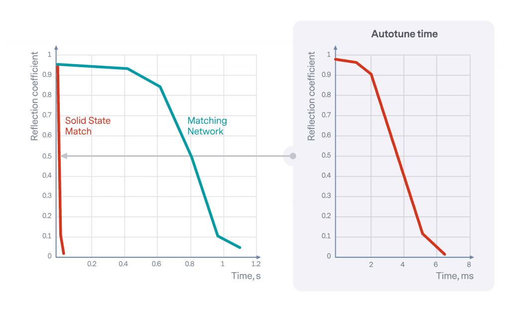
Driven by the need to achieve fast, accurate tuning across wider impedances, the integrated solid-state match solutions in cyclical deposition processes have been adopted into full-featured, stand-alone matching networks. Having similar form, footprint and tuning ranges as their traditional counterparts, these matches offer tuning times in the millisecond range compared with the one-second range typical of traditional matching networks. Illustrating this speed enhancement, tuning time of a solid-state match is compared with a variable vacuum capacitor match in FIGURE 4.

Solid-state matching networks (SSM), when configured for full-range tuning, can cover an impedance space essentially identical to that of a vacuum capacitor match while the compactness of solid-state circuitry allows the SSM to fit within a similar footprint of the conventional version (FIGURE 5). Further, SSM units have no moving mechanical parts. This eliminates wear and drift mechanisms inherent to traditional matches, enabling higher reliability and repeatability on a broad range of challenging and continually varying plasma processes.

With SSM tuning networks, accurate power delivery and tuning into critical, power sensitive, short duration plasma Etch steps are possible while still supporting the conventional longer steps and wide tuning range traditionally handled by vacuum capacitor based matching networks. Large and abrupt impedance swings, increasingly common in today’s challenging 3D device Etch processes, can also be managed by merging fast switching with novel control algorithms. With these together, tuning speed and span combine to ensure consistent power delivery through process step excursions avoiding power delivery interruption and even “winking-out” of the plasma, sometimes seen in slower, vacuum capacitor-based designs. This new approach to impedance matching addresses a myriad of new challenges presented to modern process power systems by todays demanding 3D and HARC etches.
In 2010, AE introduced the first true, wide range solid-state match (Navigator II FastCap) [1] for semiconductor plasma processing applications. With millisecond tuning times, the Navigator II FastCap found initial interest in demanding high-speed matching applications like Conductor Etch, PECVD, and Metal Deposition processes because of its ability to ensure precise and repeatable power delivery through very short duration and very fast-changing plasmas. As process step times continue to contract, demand for solid-state-matching is growing and driving wider adoption of AE’s even faster solid-state matches.
Narrowing ion energy distribution with non-sinusoidal (Non-RF) power
As discussed in the prior article, the complexity in 3D device manufacturing and High Aspect Ratio (HAR) features has driven the need for process power systems to provide better discrimination of targeted ion activation and control of the overall plasma environment. Specifically, the mix of ions to radicals, the energy distribution of ions incident to the wafer and respective arrival rates of various species (flux) are all key factors determining both quality and efficiency of these challenging 3D Etch process applications.
Multi-frequency pulsed RF power systems are now mainstream largely for their ability to separate, or decouple, plasma density production (determining flux) from ion energy generation. The ion energy distribution is an especially critical factor in HAR Etch applications. Balancing High Frequency (HF, usually 13 MHz or higher) and Mid Frequency (MF, usually 300 kHz to 2 MHz) power provides process engineers more control over ion energy distributions compared to single-frequency pulsed RF power systems. However, the time-varying character of RF biasing is emerging as a significant limitation to the scaling of these features even with dual or multi-frequency pulsed RF power.
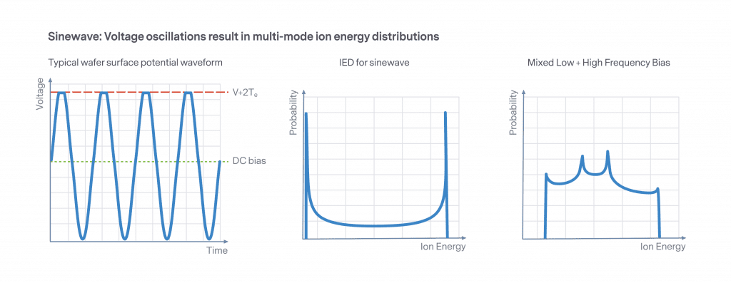
The sinusoidal nature of RF biasing produces broad, multi-peaked Ion Energy Distributions (IEDs) as seen in FIGURE 6. As described in the previous article, mixing HF with MF power balances plasma creation with high ion acceleration. To achieve the energies required in some of today’s demanding Etch processes, increasing amounts of MF power is required. However, MF power is rising to difficult to manage levels, making controllable and/or narrow IEDs even harder to achieve. Higher MF also drives higher thermal loading, along with lower efficiencies since larger fractions of applied bias is consumed by, accelerating ions to energies not adequate for and even detrimental to the process.

As 3D IC devices increase the number of layers and features get deeper, there will be a point where it becomes impractical to use conventional multi-frequency power delivery systems. The lack of adequate IED control and the trend towards higher and higher powers are problematic, leading to the need to explore alternate process power solutions for HAR biasing. A non-sinusoidal bias source has emerged as an advantageous alternative. This non-RF approach provides the means for direct control of bias voltages offering a leap forward in both efficiency and in the control of IEDs for complex and demanding applications such as 3D Etch, HAR Etch, and deposition applications.
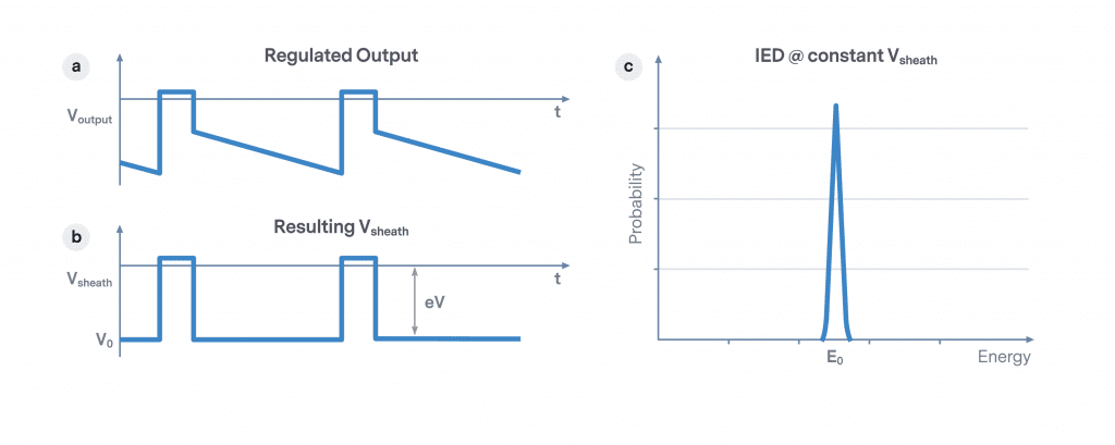
More fundamentally, to control the distribution of ion energies to a substrate, the voltage across the plasma sheath above the substrate must be carefully controlled. Since dielectrics are present on both the wafer and electrostatic wafer chuck, a form of AC voltage is required. Asymmetric waveforms, when properly regulated, have been shown [2] to provide a controllable voltage drop across the sheath and therefore controllable ion energies to the surface. To achieve direct control of the IED, an asymmetric bias approach must accomplish three key tasks: 1) establish the accelerating (sheath) voltage at the surface; 2) maintain the sheath drop at a desired level; and 3) periodically reverse to remove charge and reset for the next cycle. FIGURE 7 shows how a preferred asymmetric waveform (a) at the output (delivered to the wafer chuck) translates to producing a controllable sheath voltage (b) and, when Vsheath is held constant, a narrow IED (c).

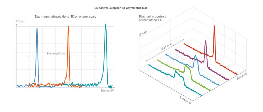
Non-sinusoidal, asymmetric bias systems are new to high-volume semiconductor manufacturing process power and offer unique advantages over conventional sinusoidal bias power approaches. Beyond the ability to produce narrow IEDs (FIGURE 8 left), they also offer the possibility to tailor energy distributions (wide or narrow) according to specific process requirements (FIGURE 8 right). Controlling the effective IED based on process objectives brings the advantage of efficiency. When bias power is more directly applied to producing only the desired range of ion energies, less power is lost accelerating ions to undesirable levels. Improving bias power efficiency not only reduces waste but also avoids the growing potential for wafer damage and premature chuck and chamber wear-out.

AE introduced eVoS™ a non-RF, asymmetric-wave bias product in 2019. Initially used in specialty applications, eVoS applications are broadening to high-performance etch and atomic-scale processes where precise control of bias and resulting ion energy distribution is required. As the novel technology scales for 3D and deep, high aspect ratio processing, the eVoS solution provides the means to increase targeted ion energy without excessively increasing RF thereby avoiding untenable levels of power and associated costs for these increasingly deep and challenging features. Benefiting from the asymmetric-wave application, eVoS provides control capabilities not available to RF (single or multiple frequency) bias systems and potentially opens new frontiers in this ever-evolving, new form of Etching.
The power of prediction
Increasingly, technology commentators claim, “data is the new oil” because of its growing value in many aspects of our daily lives. In the past few years, however, it has become clear that collecting and saving data for data’s sake alone does not add much value. However, when domain knowledge is combined with these data, it becomes possible to add huge value by identifying the “needle in the haystack” and thereby enables useful insights to be extracted from an overwhelming sea of data. In semiconductor manufacturing, the intersection of process power engineering expertise with advanced data science methodologies is where value creation happens, empowering delivery of highly differentiated value by improving process performance and results.
The objectives to deliver data-driven, actionable insights are primarily to 1) contribute to reducing the total cost of ownership; and 2) more rapidly, and with more certainty, diagnose yield and defect containment challenges. Unique to process power, and AE specifically, AE’s power generators and matching networks can be used directly to collect information that enables AE analytics without the need for additional external sensors.
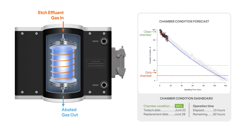
An illustrative process performance solution is predictive chamber reconditioning for point-of-use plasma abatement (of effluent process gases in semiconductor manufacturing). For this application, the chamber in a remote plasma source, used to break down the process gas byproducts downstream of the process chamber, wears over time and ultimately degrades the performance of the plasma abatement itself and requires servicing to return to targeted performance.
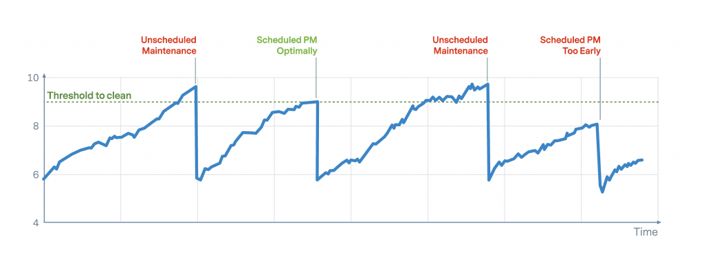
The typical preventative maintenance approach is a fixed-time intervention, such as monthly cleaning/reconditioning depending on the estimated usage. As illustrated in FIGURE 9, fixed-time maintenance is often not optimal. Sometimes, the cleaning of the chamber is done prematurely (wasting money), and sometimes it is too late, impacting process performance or worst-case causing process drift, resulting in unplanned downtime to service the plasma abatement chamber. In high-performance fabs, there is little tolerance for unexpected maintenance events that reduce productivity and raise costs.

In contrast to time-based maintenance cycles, AE developed a predictive chamber clean solution (PowerInsight by Advanced Energy™) [3] that alerts the user when the chamber should be cleaned, based on real-time usage conditions, regardless of gas species breakdown, the previous cleaning cycle, or the starting condition of the chamber. Put simply, the predictive power methodology, deployed as a Machine Learning solution and integrated into customer platforms, provides a figure-of-merit annunciation for chamber condition status and time-to-servicing (FIGURE 10).

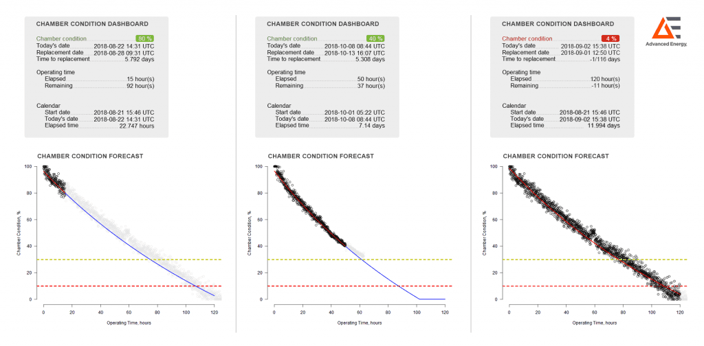
In FIGURES 11A, 11b and 11c, the figure-of-merit trend as the number of hours left to chamber cleaning is shown. The yellow line is the threshold for warning, and the red line indicates when cleaning/chamber reconditioning must be done. AE’s process power knowledge in combination with proprietary data analytics provides unique value differentiation to customers to optimize process performance and maintenance cycles.

With the explosion of Big Data, analytics, and the exponential rise of computational power, fabs are increasingly dedicating resources to use Artificial Intelligence (Machine Learning or Deep Learning) to extract actionable insights for improving productivity and yield. AE’s solutions are enabling the “last mile” of actionable insights, marrying the physics of process power applications to big data analytics. Feedback from end users (fabs) is increasingly validating this approach as a wider range of applications are adopted.
Out from the shadows to power ahead
Sub 7 nm technology nodes drive new process requirements which, in turn, demand new power solutions. Going forward, a bigger process power toolbox is being used to overcome challenges such as speed of response, ion energy distribution, and enabling measurement and control with predictive insights. These new solutions are being adopted in ways that deliver these advanced capabilities at low costs and compact sizes, as power continues to be a leading process enabler.
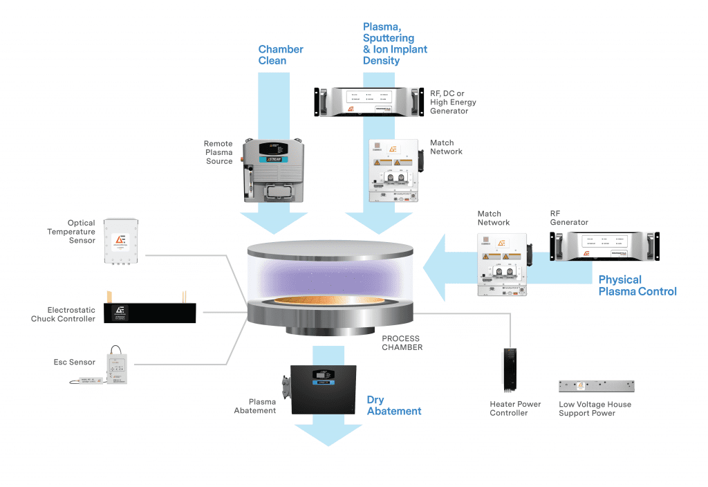
Process power control and system-wide synchronization is becoming critically enabling. In FIGURE 12, semiconductor Wafer Fab Equipment (WFE) process power elements are shown for plasma-based processes. The core importance of power also applies to Ion Implantation and E-Beam inspection and SEM processes, where high-voltage power is fundamental to controlling electron-beam performance. Temperature control and measurement is also shown due to its tight coupling with the process power delivery.

It is interesting to think that this series of articles on process power has most likely been read from remote locations as many in our industry work from home. Ironically, this shift to working from home has increased the demand for data services, which has driven the need for more compute, storage, connectivity, telecommunication, and data capacities. This, in turn, has driven the need for more high-performance computing and memory chips. This, finally, brings things full circle back to the advances in process power that are enabling chip manufacturing steps.
Many of us working from home are also newly remotely linked to our work development facilities and labs. This has additionally sped adoption of Machine Learning and Artificial Intelligence as we have used IIoT devices to interact with our equipment, provide predictive insights and even optimize our systems from a distance. This, too, is mirrored in process power as more demanding requirements and higher complexity is increasing reliance on using power parameter information to predict and optimize processes – and making advanced semiconductor manufacturing possible.
References
1. Associated Patents include US Patent 8416008B2
2. Wendt, et. al., J .App. Phys, 88, 2, 2000
3. Patent pending. Chamber clean is one of many applications that leverage PowerInsight by Advanced Energy.