KAR YEE TANG, Senior Product Marketing Manager, eSilicon, San Jose, CA
Service providers and hyperscalers –– Amazon, Apple, Facebook, Google, Intel and Microsoft –– are moving from 100 to 400 gigabit (Gb) Ethernet rates and beyond. Wireline and wireless networks are driving new architectures to support the move from 4G LTE to 5G infrastructure driven by increasing global IP traffic as the world becomes more connected digitally.
At the same time, the cloud and data centers are decentralizing as hundreds of scaled-down micro data centers are appearing at the edge of the network to support latency-sensitive IoT devices, real-time safety systems and autonomous vehicles. Other trends, including AI, smart cities and surveillance technology, help fuel this transition.
How does the semiconductor industry respond? By doing what it always does –– innovate.
Take SerDes, for example. SerDes interfaces facilitate the data transmission across the network. As traffic on the network increases and new standards emerge, SerDes designers continue to evolve the architecture and innovate, but it’s no easy task.
High-speed serial links: Arteries of Ethernet and 5G wireless
It all started with high-speed serial communication links. Through the decades, digital communication buses transitioned from parallel to high-speed serial buses, from single to multiple serial lanes and from one to 112Gbps transfer rates.
Next-generation servers, switches, routers and 5G infrastructure will place unprecedented demands on a SerDes PHY for increased speed, signal quality, power efficiency and scalability to satisfy the need for more data faster.
As new 5G frequency bands and modulation schemes bring higher data rates and lower latencies, base stations need to support higher transfer rates per user, more users per site and more data streams per user. This stresses the front haul link between the radio remote unit (RRU) and the base band unit (BBU), pushing the SerDes PHY between the RRU and BBU to support common radio interface (CPRI/eCPRI) rates up to 25Gb/s today and beyond 50Gb/s tomorrow.
More than that, the wireless infrastructure presents a unique paradigm –– chasing leading-edge technologies while remaining cost-sensitive and leveraging economies of scale.
The data center market has been at the forefront of technology. Now, the SerDes PHY must meet long-reach backplane requirements and scale from 28G to 56G and 112G to support the transition to 25.6 and 51.2 terabit switches. Network architects are facing an increasing number of SerDes lanes with between 300 and 500 or more channels per line card to the fabric. A 56G SerDes PHY can support 100G, 200G and 400G Ethernet standards with two, four and eight lanes. System designers can reduce the number of lanes or achieve double the Ethernet rates with a 112G SerDes PHY.
While short-reach SerDes was ideal for chip-to-module and chip-to-chip interfaces, its application space is shrinking as rates increase to 56 and 112Gb/s. As well, long-reach capabilities increasingly are needed for one meter or more chip-to-backplane interfaces and to drive copper cables with lengths exceeding three meters to connect servers to the top-of-the-rack switch.
SerDes today must be able to support each unique requirement under separate conditions for chip-to-chip, chip-to-module and chip-to-backplane connectivity.
Signal integrity challenges and innovation
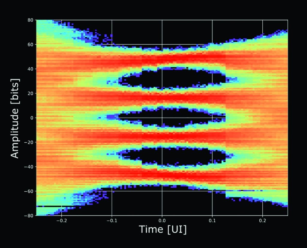
Preserving good signal integrity and holding a low bit error rate (BER) at increasing channel insertion loss (IL) is a challenge moving from short- to long-reach links and from 28Gb/s to 112Gb/s link rates. At higher rates, the bandwidth provided by NRZ/PAM2 is no longer able to hold rates beyond 28Gb/s. PAM4 was adopted for higher rates because it requires half the Nyquist frequency of PAM2 for the same throughput. However, PAM4 signals are only one third of PAM2 height, giving it a lower signal-to-noise ratio (SNR) and adding further penalty to insertion loss alone. A good serial link supporting 56G and beyond must be optimized for insertion loss in excess of 35dB (Figure 1).

At such high rates, every section along the high-speed serial path from the transmitter to the receiver must be tuned for the best signal integrity and quality. Because the transmitter is usually the source of deterministic jitter, having a low-transmit random jitter is essential –– typically no more than 150fs for 112Gb/s operation.
When high-speed signals travel over long PCB traces, connectors and cables, signal quality is impacted by high levels of insertion loss and crosstalk, trace densities and interference between the lanes.
Advanced equalization techniques on the transmit and receive sides must be designed to compensate for these effects, especially across the backplane. The receiver must support different frequency boosts at Nyquist to improve link margin and avoid signal distortion. The transmit feed-forward equalization (FFE), on the other hand, needs to be programmable with several pre- or post-cursor taps for maximum flexibility when extending channel reach.
For system independence, separate Tx and Rx clock sources are necessary to allow individual speed settings on every lane to provide full flexibility to the network architect. This enables independent training and auto-negotiation on a per-lane basis to accommodate different upstream and downstream data rates. Advanced clocking schemes that allow a large selection of reference clock frequencies in addition to the classical references of 156.25 and 212.5 megahertz are crucial.
Maintaining an unlimited range of data rates is important when supporting multiple standards with one SerDes PHY –– mixing Fibre Channel and 100GBase-KR4 as four lanes each in one eight-lane SerDes macro, for example. A robust SerDes PHY should support hole-free data rate coverage for backward compatibility with legacy standards while stretching the coverage to achieve next-generation systems. For PAM2/NRZ operations, the hole-free data rate coverage should extend from one to 30Gb/s, and up to 60Gb/s for PAM4 operations.
Complex architectures for such extreme speed require more advanced on-chip test capabilities for accurate real-time monitoring beyond IC-level simulation and modeling. Full-speed internal analog and digital loopback capabilities, coupled with smart monitoring features including signal-to-noise ratio (SNR) calculations, per-eye BER calculations, non-destructive eye diagrams, bathtubs and histograms, can simplify and accelerate system validation (Figure 2).

Moving ahead
While every application conforms to a different list of standards with specific requirements, SerDes designs must evolve to keep pace with the demanding network environment. As speed, signal integrity and test boundaries are pushed, cycles of architectural changes and new levels of design innovation for the SerDes chip are only a few of the challenges. Demonstrating SerDes’ capabilities in silicon in and out of the lab is the challenge to prove its value.