Jim O’Neill and Jun-Fei Zheng, Entegris, Billerica, MA
As new applications for smart devices, 5G communication, and artificial intelligence gain traction, the demand for high performance logic devices and high-density memory increases. The necessary improvements in computational speed and data bandwidth require new device architectures such as narrow FinFETs or stacked nanowire transistors. Such structures can only be enabled by new materials that not only meet the performance requirements of the device but also have specific properties that allow them to be applied to the challenging geometries that are involved. Each change in material in one portion of the fabrication process has a cascading impact on the subsequent steps that may affect yield, reliability or cost of the chip. Successfully integrating a new material into the device building process requires a clear understanding of all the downstream implications and process challenges. Therefore, a holistic approach to new material integration is required. Let’s explore this further.
Logic FEOL integration challenges
Transistor advancement began with shrinking the gate length and then changing gate materials. Replacing SiO2 with high-k dielectrics and polysilicon with metal gate materials reduced the effective oxide thickness, improving switching speed and reducing off-state leakage. For even higher performance, changes in materials alone do not sufficiently improve speed and reduce off-state leakage. The next steps require changes in device geometry (Figure 1).

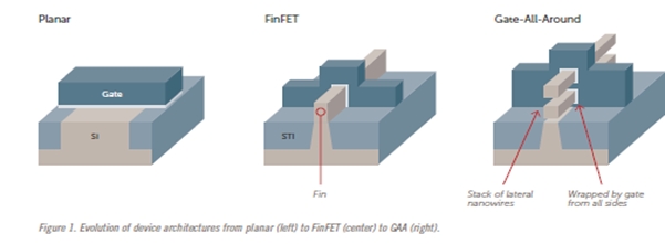
The first step in this evolution was to migrate from planar devices to FinFET gate structures, with a vertical gate configuration in which a high-k dielectric and a metal gate wraps around the fin-shaped channel to provide greater surface area to allow for higher channel currents in a compact footprint. Producing taller, narrower fins or incorporating multiple parallel fins extends the FinFET architecture to more advanced nodes, including 22, 14, 10, 7 nm and potentially 5nm. As gate dimensions shrink below 5 nm, however, even the FinFET may reach its limits.
The next step for improving scaling the gate architecture is a gate all around (GAA) structure, where nanowires coated with gate dielectric and metal layers provide 360 degrees of channel surface coverage. Wrapping the gate stack around the channel improves static electrical field control and provides better sub-threshold slope control of the on/off charge flow in the nanowire channel. The GAA structure may require multiple stacked nanowires to provide sufficient on-current for high-speed performance at a given footprint. Nanowire structures represent the future of logic integration, but they pose many materials and processing challenges, including parasitic capacitor control challenge.
Producing nanowires
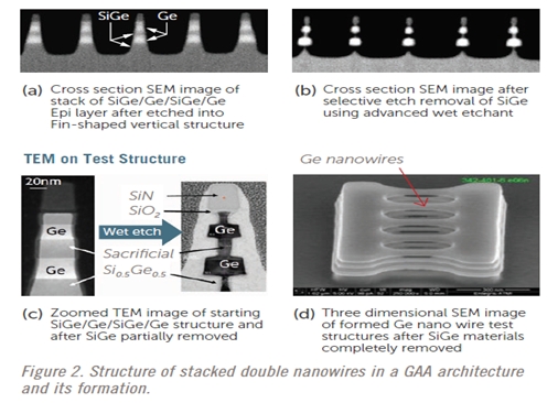
Starting with a vertical fin structure consisting of alternating silicon/silicon-germanium (Si/SiGe) or germanium/silicon-germanium (Ge/SiGe) layers (Figure 2a), the SiGe is selectively etched away by a wet chemical formulation to form Si or Ge nanowires (Figures 2b, 2c and 2d). The choice of Ge versus Si depends on the application. Si is the conventional option for channel material, but for the 5 nm node and beyond, Ge channel materials with greater hole mobility will be needed to increase PMOS transistor speed.

Germanium-based nanowire transistors
Ge provides greater hole mobility than Si, but its smaller bandgap can cause off-state current leakage. Fortunately, the GAA structure helps to limit such leakage, making Ge especially attractive. Low operating voltage, often chosen to reduce power consumption, also favors Ge selection.
Regardless of the chosen semiconductor channel material, selective wet or dry etching to release the nanowires poses a considerable challenge. Etch chemistry must be carefully tuned to remove the SiGe without attacking the Ge nanowires.
While Ge is the preferred semiconductor for GAA structures, the instability of Ge oxides existing at the interface of Ge and high-k dielectric poses a problem. Special clean formulations for Ge-based channel surfaces are required to reduce interface defect density. Doping at the sequential high-k gate dielectric is one approach that may stabilize Ge oxides and thus reduce defects at the interface.
The exposed nanowires then require conformal deposition of high-k dielectrics and metal gates (Figure 3). Uniformly coating the surfaces of multiple nanowires with nm-scale gate films is more difficult than coating vertical fins. Conformal coatings of gate dielectrics and metal films to form a gate stack only a few nanometers thick around the nanowire channel requires nearly atomic-level control of the deposition process.

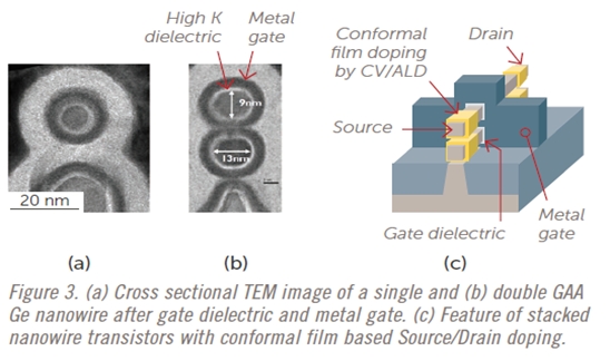
The source and drain ends of the nanowire transistors cannot use standard doping techniques such as vertical implant, because the dopants cannot reach the bottom surface of the nanowires due to shadowing. Plasma doping can reach the sides of each nanowire but not the entire surface of the structure. So new conformal source and drain doping methods must be developed.
BEOL challenges: Revisiting interconnect materials
As the transistor shrinks, conventional copper (Cu) interconnects are reaching their scaling limits. The metal line resistivity increases sharply as the width become comparable with the line edge roughness and Cu grain size due to increased electron scattering at grain boundaries and surfaces. In addition, the highly resistive liner and barrier take up a more significant fraction of small lines thereby increasing line resistance drastically for dimensions below 10-20 nm.
Swapping interconnect materials, including metallurgies that require thinner liners are currently major efforts in back-end-of-line (BEOL) processing. Substituting cobalt (Co) for W contacts and small Cu interconnects is one path that has been explored [1]. The use of W and Cu require a minimum barrier thickness to prevent unwanted diffusion and degraded reliability. However, Co requires a thinner barrier layer translating to a greater conductive volume of Co and lower resistivity. Cobalt has another advantage in bottom-up, selective fill can be achieved enabling void-free high aspect ratio vias [2]. Alternative metals such as ruthenium (Ru), molybdenum (Mo), and many more are also being tested. However, the integration of such materials requires changes in metal precursors for deposition, plating formulations as well as polishing and cleaning chemistries.
CMP and post-CMP clean chemistry
Co requires a different barrier layer configuration than Cu — titanium and titanium nitride (Ti/TiN) instead of tantalum nitride/tantalum (TaN/Ta). With this, the entire electrochemistry changes and so must the composition of etchants and cleans. The components of critical formulations must be tailored to the metal system.
Cleans after CMP are especially critical [3], and new formulations have been developed for use with Co metallization (Figure 4). In this system etchants dissolve the Co oxides to free silica (SiO2) particles, while organic additives attack and remove organic residues. Adding a corrosion inhibitor controls galvanic corrosion during the clean process.

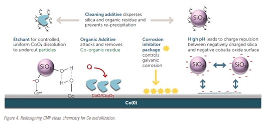
Additional additives disperse the SiO2 and organic residues to avoid reprecipitation, but these additives only work well in a narrow pH range. High pH is necessary to increase charge repulsion between the SiO2 and Co oxide to more effectively remove the negatively charged silica particles from the surface. Therefore, the pH of the clean solution needs to be carefully controlled to minimize the risk of SiO2 redeposition or precipitation of Co hydroxides.
Changing clean chemistry affects other aspects of the process as well. For example, it is important to consider how the new clean formulation will interact with chemically functionalized membranes used in advanced filter devices resulting in significant contamination and yield implications. The presence of different chemical species and contaminants may require changes in membrane or filter design.
Future materials integration challenges
For nanowire architectures and appropriately scaled metal interconnects to move from R&D to high-volume production, the semiconductor industry will need to tackle several challenges to create reliable, high-yielding nm-scale structures tailored to each specific application. Developing advanced precursors and associated delivery methods, enabling selective deposition of metals and dielectrics, and achieving conformal semiconductor materials doping are among the many efforts.
Solid precursor delivery
Reliable ALD and CVD deposition for nanoscale and nanowire structure demands appropriate precursors. Standard precursors, which are typically gases or liquids at ambient temperature, are extensively studied but not necessarily ideal for the conformal deposition that nanowire structures require. Process designers need the flexibility to consider as many viable precursors as possible.
The ideal precursor molecule may, in fact, be a solid at room temperature, requiring specialized vessels for delivery. Solid tungsten pentachloride (WCl5), for example, is a good precursor for CVD W, replacing gas phase tungsten hexafluoride (WF6) for a fluorine-free CVD process. A halide precursor, hafnium chloride (HfCl4), is also a solid preferred for gate dielectric applications to avoid the carbon impurities generated when metal-organic precursors decompose.
When heated for delivery, HfCl4 sublimates instead of melting. A carrier gas is required for efficient delivery and care must be exercised to avoid introducing unwanted contaminants—either solid particles from the precursor itself or metal impurities resulting from chemical interactions between the precursor and the metal vessel. Such contaminants pose a substantial risk of device failure or reduced reliability in the field.
Advanced gas filtration appropriate for low vapor pressure applications is needed to allow sublimated precursor to pass through while restricting the flow of contaminants. Aspects of such specialized filters such as pore size, filter material, and filter morphology must be optimized for the specific precursors involved and the type of potential contaminants present [4]. Specialized coatings applied to the inside of the filter has proven to be very effective to avoid metallic contamination.
Selective deposition
Complex geometries, including extremely small trenches and holes, pose a substantial challenge for filling the structure without a seam or void. Electrochemical plating with bottom-up fill characteristics has been successfully demonstrated. Alternatively, selective metal-on-metal deposition is another approach to achieve seam- and void-free fill with pure metal without the possible impact of incorporating impurities during plating.
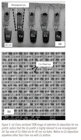
In the BEOL, Co may show considerable promise in solving the void or seam issue in nanometer dimension vias. Certain Co precursors will selectively deposit onto a metal interface at the bottom of the via without attaching to the dielectric on the sidewall or top surfaces [4]. This efficient bottom-up via fill process creates void-free, extremely small, self-aligned Co pre-filled structures. The process is forgiving, allowing for minor misalignment. Co is a proven interconnect metal that already serves as a gate contact metal, which makes it an attractive choice. Other metals, such as Ru and Mo, are also under evaluation for selective deposition applications (Figures 5a and 5b).

Cleaner materials are the key
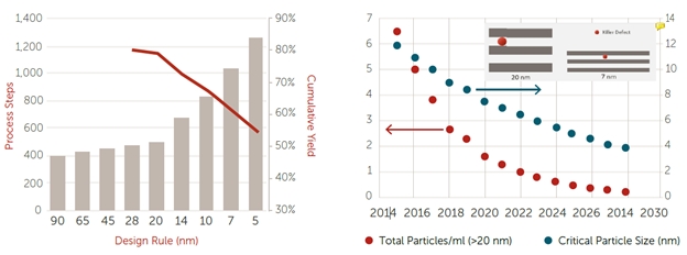
As new materials have been introduced to the chip fabrication process below the 28nm node, the number of process steps has increased significantly making yield ramps increasingly difficult (Fig. 6a). As the metal line and pitch shrink, the size of critical defects decreases as does the total acceptable particle count (Fig. 6b). The importance of material purity and overall defect control becomes enormously important.

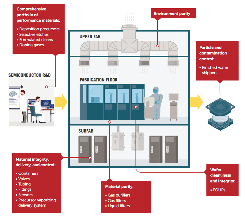
Entegris not only supplies the fab advanced deposition precursors, formulations for advanced cleans and etching processes, and gases for advanced doping applications, it also ensures the integrity of those materials from the point where they are created to where they are used on the wafer. This includes liquid and gas filtration and purification, material packaging and delivery, environmental cleanliness and process control (Fig. 7). Furthermore, it provides the ability to handle and transport finished wafers to another line, such as wafer level package area, for continued processing. Entegris has the ability to optimize all these capabilities to support advanced node device builds holistically enabling aggressive yield improvement and cost control.

Summary
The complex processes required to build advanced logic and memory devices require new materials to enable the challenging geometries that are involved. The integration of one material in a specific point in the fabrication process affects subsequent steps in the build. The successful introduction of a single new film to improve one aspect of the device performance requires a clear understanding of all potential downstream implications.
So how can you best address this? Taking a holistic approach to materials integration considering the subtle effects of seemingly simple materials challenges is required to ensure performance, yield, reliability, and overall cost of ownership, which ultimately leads to success in going to market.
References
1. Croes, K, et al., “Interconnect metals beyond copper: reliability challenges and opportunities,” Proc. IEEE International Electron Devices Meeting (IEDM), 5.3.1, DOI: 10.1109/IEDM.2018.8614695 (2018).
2. Zheng, J-F, et al., “Selective Co Growth on Cu for Void-Free Via Fill,” IEEE International Interconnect Technology Conference and IEEE Materials for Advanced Metallization Conference, L265 (2015).
3. White, M., et al., “Mechanistic and Electrochemical Aspects of Copper and Cobalt Post CMP Cleaners for 5-7 nm Nodes,” Surface Preparation and Cleaning Conference (SPCC), Linx Consulting (2017).
4. Ozzello, A., “Empirical model to understand particle removal behavior during bulk chemical filtration,” Ultrapure Micro, Austin, TX, May 30-June 1, 2018.