By RAJ MELKOTE, VP Engineering, Semiconductor Chamber Solutions, Edwards Vacuum, Chelmsford, MA
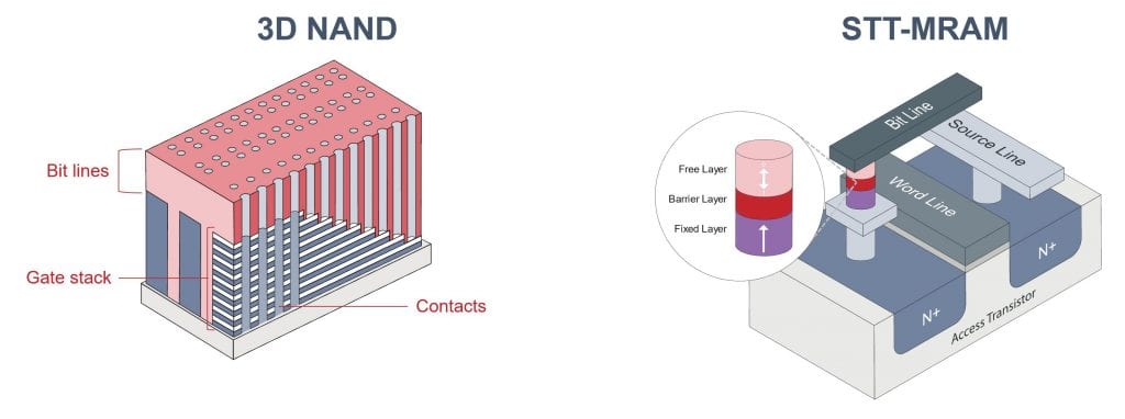
High Aspect Ratio (HAR) etch is fast emerging as the dominant method for fabricating next generation silicon micro-structures in devices such as 3D-NAND and STT-MRAM (Figure 1). As these and other technologies scale further, achieving anisotropic HAR etch at commercially feasible yields and process times is a paramount challenge. Etching at cryogenic temperatures has a number of advantages in HAR applications but advancing process requirements are driving the need for colder wafer temperatures and better particle control.

Introduction
First introduced in the 1980s [1], cryogenic etching has gained momentum recently as production of devices like 3D-NAND, which incorporate very high aspect ratio (HAR) features, has grown significantly. The high directionality and selectivity of cryo-etch allow it to create higher aspect ratio features with fewer process steps than other methods. Current cryo-etch processes require wafer temperatures below -87°C. Accounting for temperature gradients, practical heat transfer limitations, and the exothermic nature of certain reactions in the etch process, this indicates a desirable process window between -110°C and -120°C. The impracticality of using liquid nitrogen to achieve these temperatures in a clean room environment is driving a search for other cooling solutions. Mixed refrigerant Joule-Thomson (MR-JT) cryo chillers (Edwards Polycold) offer advantages in energy consumption, physical footprint, and reliability, and can be an ideal solution for HAR cryogenic etching.
In addition to meeting the cooling challenge, manufacturers using advanced etch and deposition processes must also address the increasing sensitivity of smaller, deeper features to defects caused by particle contamination. For atomic layer processes used to create the smallest structures, controlling particles is a key requirement in managing defectivity and yield. Particle formation during multi-layer plasma etching is mediated by the presence of water molecules, and the number of particles generated has been shown to be directly related to the partial pressure of water vapor in the chamber [2]. In-chamber cryo-trapping can reduce water vapor partial pressure. The number of particles is also affected by the design of the turbomolecular pump used to evacuate the chamber. Particle transport models have shown that particles can recoil back into the chamber from rapidly spinning turbomolecular pump rotors. Refinements in pump design can reduce the number of recoiling particles. Combining enhanced cryo-trapping and turbomolecular pumping technologies has the potential to significantly reduce particulate contamination and associated yield losses.
HAR structures and the need for cryogenic etch
As gains in areal density become more difficult and expensive, semiconductor device manufacturers have gone vertical, creating complicated three-dimensional designs as they strive to pack more computing power and functionality into less space. Some of these devices use features with extremely high aspect ratios. For example, 3D NAND devices already in production use features with aspect ratios greater than 60:1. In some cases, such as the contact lines that connect stacked memory cells, the feature starts a straight vertical hole that is subsequently filled with a sequence of various materials to create a column with multiple concentric layers. Etching the original hole, which must be straight and of uniform diameter, requires an etch process that is highly directional, removing material efficiently at the bottom of the hole but not from the walls. The process must also be highly selective, to remove material from the hole while not eroding the mask that defines the hole’s diameter and position. In other cases, as when creating the trenches that separate rows of columns, the etch processes must remove material both vertically, to create the trench, and laterally, to remove material from between layers in the stack, requiring again both directionality and selectivity. The etch and deposition processes used to create these complex structures are themselves very complex, often involving the use of atomic layer techniques that remove or deposit one atomic layer at a time. Atomic layer processes proceed via a sequence of alternating steps, with one step preparing the surface layer for the next step which removes or deposits a single atomic layer. Atomic layer processes put high demands on the vacuum system, which must completely exchange gases in the chamber between alternating steps. Anything that accelerates the exchange can have significant impact on productivity [3].
Cryo-etch processes use very low temperatures to enhance their directionality and selectivity. As shown for silicon etch in Figure 2, the etch rate for silicon increases dramatically at lower temperatures, while the etch rate for silicon dioxide and photoresist decreases. Similar differences in etch rates exist for other materials as well. High selectivity can improve directionality. Energetic ions remove material efficiently from the bottom of the hole while a passivation layer, which etches more slowly and receives only glancing ion collisions, protects the walls from etching in the lateral direction, reducing edge defects and scalloping. The sidewall passivation layer (SiOxFy) desorbs at higher temperatures, reducing overall process steps. Very low lateral diffusion (O2 or similar) further eliminates the need for damage repair process steps. High selectivity also reduces erosion of the photoresist or hard mask that defines a feature’s shape and position. The net result is higher aspect ratio features with fewer process steps.
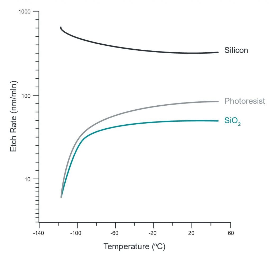
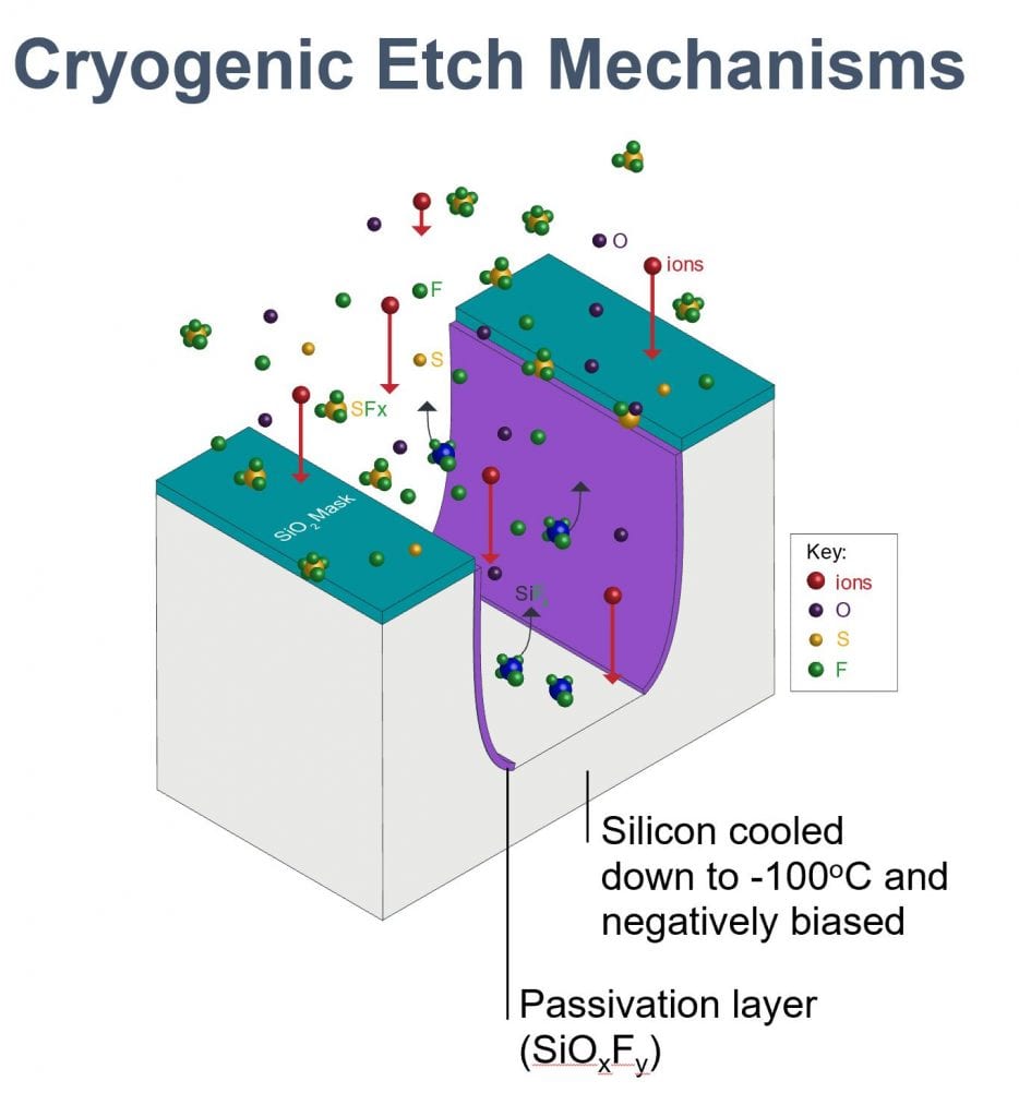
Figure 2. Etching at cryogenic temperatures provides improves selectivity and directionality. Excellent sidewall passivation during etch minimizes sidewall scalloping and edge defects.
However, cryo-etch puts a new set of demands on process equipment to generate low temperatures and sufficient cooling power. 3D-NAND applications need wafer chuck temperatures between -80°C and -140°C with power ranging from 8kW to 15kW. STT-MRAM temperature requirements are between -140°C and -200°C, with power up to 2kW. The system should be closed loop, to reduce operating costs, and the cooling fluid must have a high dielectric strength. The system must be able to cool (and heat) a rotating wafer chuck and provide multiple cooling circuits to condition different components of the process and pre-process chamber. Finally, it must provide tight temperature control (+/- 1°C) for process uniformity and repeatability, and good set-point resolution, for process tunability.
Traditional chillers in semiconductor manufacturing applications use glycol-based coolants and multistage compression to provide temperatures down to about -70°C. Next generation processes will require mixed-refrigerant Joule-Thomson (MR-JT) cryo-chillers, which can deliver temperatures as low as -170°C. Temperatures beyond that will likely require a different technology, perhaps Gifford-McMahon refrigeration.
MR-JT cryo-chillers use a process similar to that found in a kitchen refrigerator or household air-conditioner. The working fluid is compressed, increasing its temperature and transferring heat to the external environment. Then the fluid is allowed to expand through an orifice, cooling as it does so and absorbing heat from the cooled space or object. Household refrigerators and air-conditioners use a pure fluid. In order to achieve much lower temperatures, MR-JT use mixed fluids specially chosen for their thermodynamic properties (enthalpy, entropy, phase diagram) to reach temperatures much lower than can be attained with pure refrigerants.
The heat removal medium (circulating between the chuck and the cooling mechanism) in semiconductor manufacturing applications requires special consideration of characteristics such as dielectric constant and material compatibility, but the dominant factor is the lowest required chuck temperature. Traditional glycol-based coolants are practical down to about -40°C. Advanced engineering coolants (often silicon-based and sometimes flammable) extend this down to about -90°C. Temperatures below this require direct refrigerant cooling (no transfer medium). Other considerations specific to semiconductor manufacturing include reliability (inversely related to system complexity), footprint, and energy consumption. While cascade chillers using multiple stages and advanced thermal exchange media can achieve temperatures down to -90°C, they are larger, more complex and less energy efficient than comparable MR-JT systems. Moreover, the MR-JT technology can deliver the temperatures and power needed for next generation processes.
Particle contamination and associated defectivity
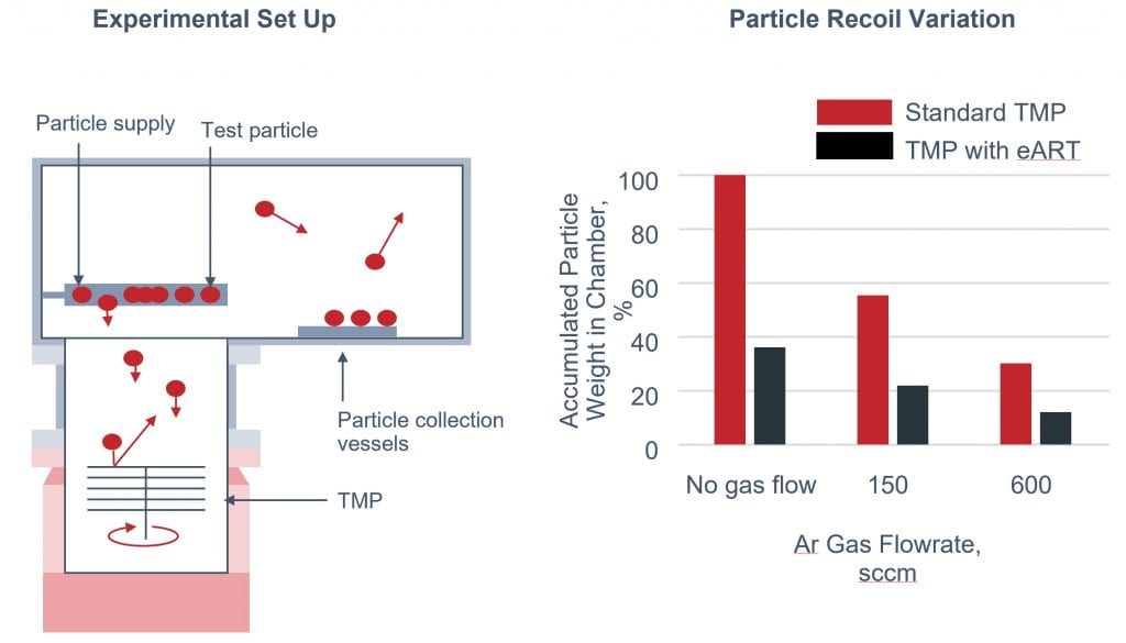
In an effort to understand the factors affecting particle contamination, Edwards engineers modeled particle capture and transport in the chamber and through the turbomolecular pump. They found that a significant number of particles, as high as 50%, actually recoil back into the chamber after collisions with the rapidly spinning pump rotor. To evaluate the effects of pump modifications, they performed an experiment, represented schematically in Figure 3, in which test particles from an artificial supply are introduced into the chamber environment and the number of particles landing on a wafer-like collection device are counted in the presence or absence of various design changes. Enhancements in materials (low sticking coefficient) and rotor geometry had significant influences. The results shown compare a standard turbomolecular pump to one that includes a set of enhancements known as EART (Edwards Anti -Recoil Technology) at various gas flow rates, showing reductions in deposited particles greater than 60% for the EART-equipped pump.

Particles also form in the chamber. Researchers in Japan investigated particle formation in plasma etching of multi-layered tungsten silicide and polycrystalline silicon [2]. They counted particles during the etch process with an in-situ monitor and determined particle composition (AlF3) with energy dispersive X-ray analysis. Ultimately, they determined that particles are formed when water in the chamber atmosphere and/or on the chamber walls reacts with fluorine in the plasma to form hydrofluoric acid (HF). The HF reacts with the aluminum oxide (Al2O3) coating on the chamber walls to form the AlF3 particles and regenerate water (H20), which is then available to repeat the cycle (eq. 1). They demonstrated a substantial reduction in particle generation when the chamber was dehydrated by plasma discharge.
- 6 HF + Al2O3 → 2 AlF3 + 3 H2O
Cryogenic trapping is another way to remove water from the process chamber. Etch process pressures are tending to lower values in the mTorr range, and base chamber pressure needs to be at least an order of magnitude lower to achieve acceptable cleanliness levels. In the sub mTorr range water vapor is the primary constituent of the chamber atmosphere. Water molecules are more difficult to pump than other gases. At low pressures, other gas molecules tend to bounce off chamber walls, each other and turbomolecular pump inlet blades (driving most of them into the pump and out of the chamber). Water vapor’s low energy level means that water molecules tend to stick to surfaces they collide with, rather than bounce off. Porous ceramic surfaces, common in process chambers also tend to absorb lots of water vapor. Adding a cryogenic pump in the chamber to trap water vapor, in series with an anti-recoil turbomolecular pump, can minimize water vapor partial pressure, lower base pressure, shorten cycle times, reduce particle counts, improve defectivity and increase yield.
Summary
As semiconductor device designers and manufacturers continue their drive to put more computing power and functionality into less space, they are incorporating high aspect ratio features fabricated with advanced etch and deposition processes. Low temperatures increase the directionality and selectivity of the etch process, allowing higher aspect ratios and reducing the number of process steps. Mixed-refrigerant Joule-Thomson refrigeration can provide the necessary wafer temperatures and cooling power with smaller footprint, better reliability and lower power consumption than alternative cooling technologies. In addition to providing cooling capability, manufacturers must address the increasing sensitivity of smaller, higher aspect ratio features to defects caused by particulate contamination. Improvements in turbomolecular pump design can reduce the number of particles deflected back into the chamber by the pump’s rotor blades. Cryo-trapping can reduce particle generation by removing the water that mediates the particle formation process. Together, these technologies will be critical enablers of next generation processes and devices.
Acknowledgements
The author wishes to recognize and thank Declan Scanlan, Market Sector Manager, Dawn Stephenson, Business Development Manager, and Kaustubh Kale, Refrigeration Technology Engineer, for the important contributions they made to this work.
References
1. Tachi S, Tsujimoto K and Okudaira S “Low-temperature reactive ion etching and microwave plasma etching of silicon” Applied Physics Letters, vol. 52, issue 8, 616, 1988.
2. N. Ito, T. Moriya, F. Uesugi, M. Matsumoto, S. Liu, and Y. Kitayama, “Reduction of particle contamination in plasma-etching equipment by dehydration of chamber wall,” Japanese Journal of Applied Physics, vol. 47, no. 5, pp. 3630-3634, 2008.
3. D. Scanlan, D. Stephenson, “Innovative Approaches to Vacuum Enable High-Volume Atomic Layer Processing”, Semiconductor Digest, July 2019, pp 26-29