By SHERIF HANY MOUSA, technical marketing engineer, Mentor, a Siemens Business
Big steel bridges like the Forth Bridge near Edinburgh, Scotland and the Golden Gate Bridge in San Francisco, California require constant maintenance. Part of that maintenance includes a constant need for repainting areas affected by water and weather to avoid rusting and corrosion. Since 1890, the Forth Bridge has required about three years to finish painting it end-to-end (Figure 1). However, by the time the maintenance crew finishes its painting on one side they need to start scraping and painting again from the beginning. “Painting the Forth Bridge” has become a colloquial expression for a never-ending task.


But change has come to the Forth Bridge. In 2011, a new coating similar to that used by the offshore oil industry was applied to the Forth Bridge to create a virtually impenetrable layer that will last for 25 years.
“For the first time in the bridge’s history, there will be no painters on the bridge every day. Job done.” Colin Hardie, Balfour Beatty Construction [1]
Do you ever feel like you’re “painting the Forth Bridge” as you tweak and revalidate your very large scale integration (VLSI) design over and over again? With the evolution in VLSI design requirements and process complexity, validation flows have become more complicated and tend to last longer. Whether the design is being optimized for enhanced functionality or improved performance, the signoff qualification process generally requires re-running all of the physical validation flows, as well as circuit validation and reliability verification flows. In each flow, metadata is repeatedly generated, even when that input design data is untouched.
For example, tweaking the design back-end (layout geometries) doesn’t impact the front-end (schematic) devices and block circuit topologies, but schematic information is still generated and verified each time. Similarly, all back-end-of-line (BEOL) layers engineering change order (ECO) and spin-off jobs include front-end of line (FEOL) layers extraction and validation, even if those FEOL layers are unchanged. All of those redundant steps directly translate into unnecessary runtime and resource overhead, which reduces productivity, increases costs, and extends tapeout schedules.
All that is about to change. Some electronic design automation (EDA) tools have introduced an innovative approach that allows designers to generate design metadata one time for certain verification flows. When checks must be re-run, that metadata is pragmatically reused to skip steps in which the data is untouched, improving both designer productivity and turnaround time (TAT). This “smart restart” metadata generation not only improves TAT for reliability verification flows, such as voltage-aware design rule checking (VA-DRC), and point to point (P2P) and current density (CD) verification, but also design for manufacturability (DFM) applications such as failure analysis and design profiling.
VA-DRC re-checking
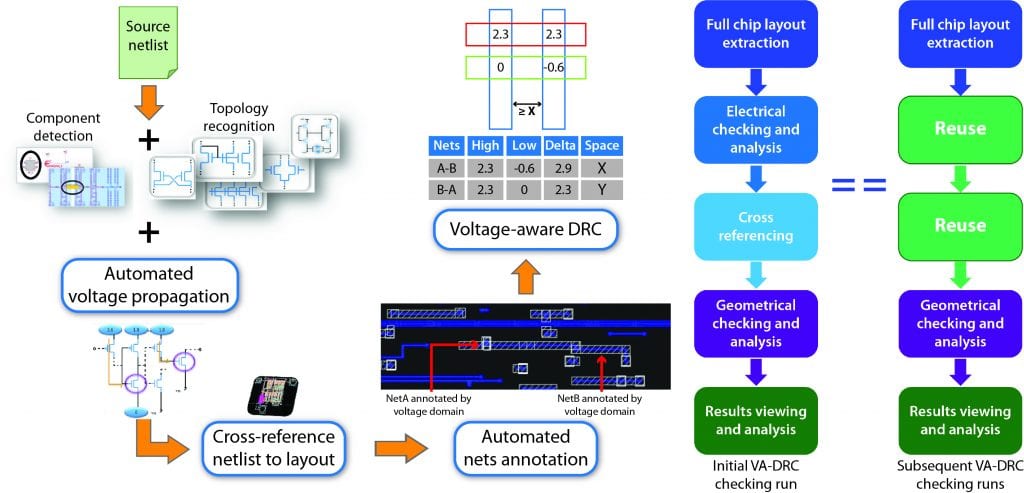
The essential element of VA-DRC is its ability to incorporate voltage information into the physical check, which is particularly useful given the growth in complex multi-voltage designs, and the need to fit more and more functionality into the same or smaller design areas [2]. EDA tools like the Calibre™ PERC™ platform, with its logic-driven layout (LDL) VA-DRC flow, can propagate voltages statically from the top ports to determine the correct voltage domain on the netlist level, cross-reference the netlist to the layout, then annotate the nets or devices of interest before cross-referencing the netlist to the layout side to perform the spacing checks [3]. This automated context-aware voltage propagation and annotation eliminates human error and improves the accuracy of VA-DRC spacing in today’s complex designs, while also significantly reducing the turnaround-time for VA-DRC verification.
However, during subsequent design rechecking, the same voltage propagation results and cross-referencing information are generated all over again, even though they don’t change. By saving the information the first time it is generated, the smart restart metadata generation eliminates the need to recreate the data in subsequent runs, saving the time required for that process while also allowing the recheck to start immediately (Figure 2).

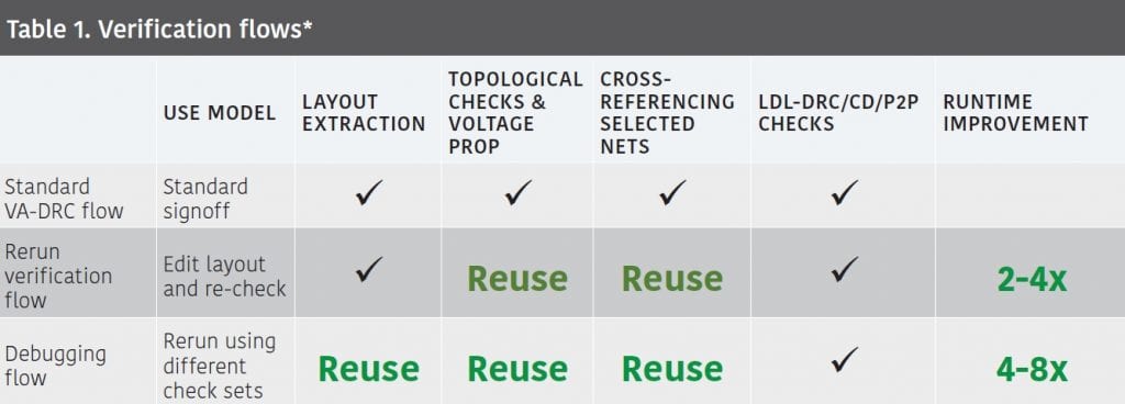
For example, let’s look at results obtained when running and debugging a typical VA-DRC flow enabling this smart metadata reuse. Table 1 shows the steps that do not have be repeated, and demonstrates the time savings available when re-using voltage propagation and cross-reference data in rechecking and debugging flows. In this case, we ran LDL-DRC context-aware geometrical checks, as well as CD and P2P checks.

DFM/Failure analysis applications
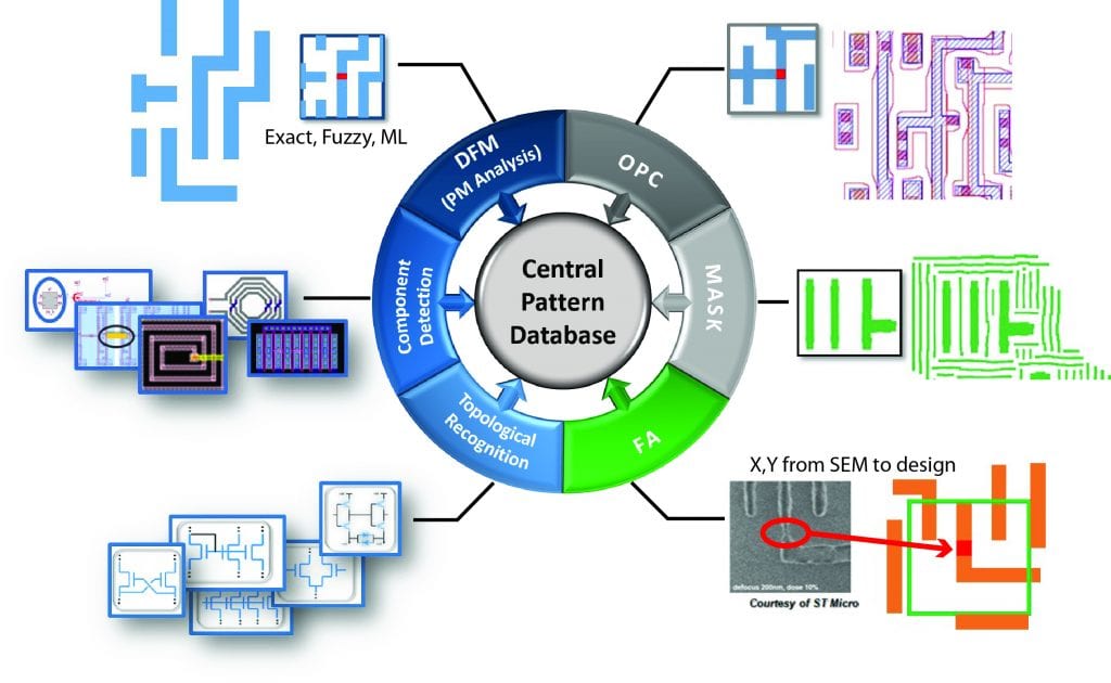
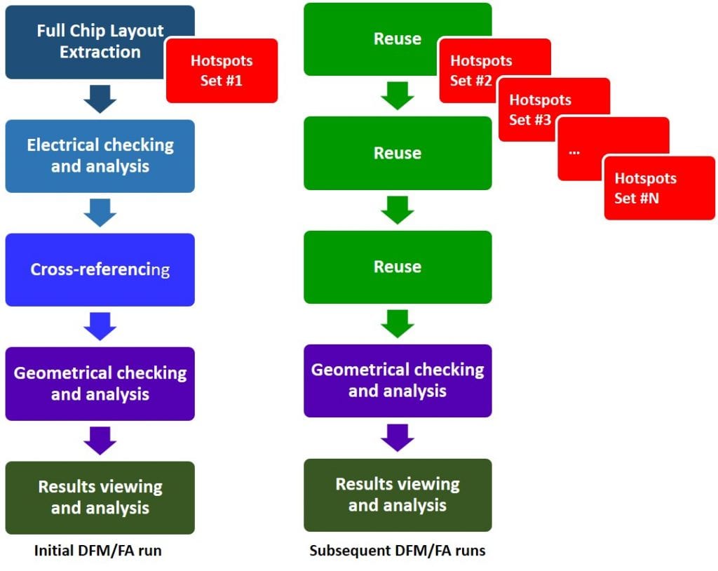
For DFM and failure analysis applications, design metadata is generated based on the design profiling (Figure 3). Metadata information comes from multiple sources, including scanning electron microscope (SEM) images, lithographic and optical process correction (OPC) hotspots, test hotspots, and DFM yield detractors. Embedded circuit intelligences, used circuit topologies, geometrical patterns representing the design style and good yielding patterns, and thousands of other metadata elements can be stored and reused many times. Not only does this reuse reduce turnaround-time, but the collected metadata also enriches the debugging and pre/post-silicon analysis.

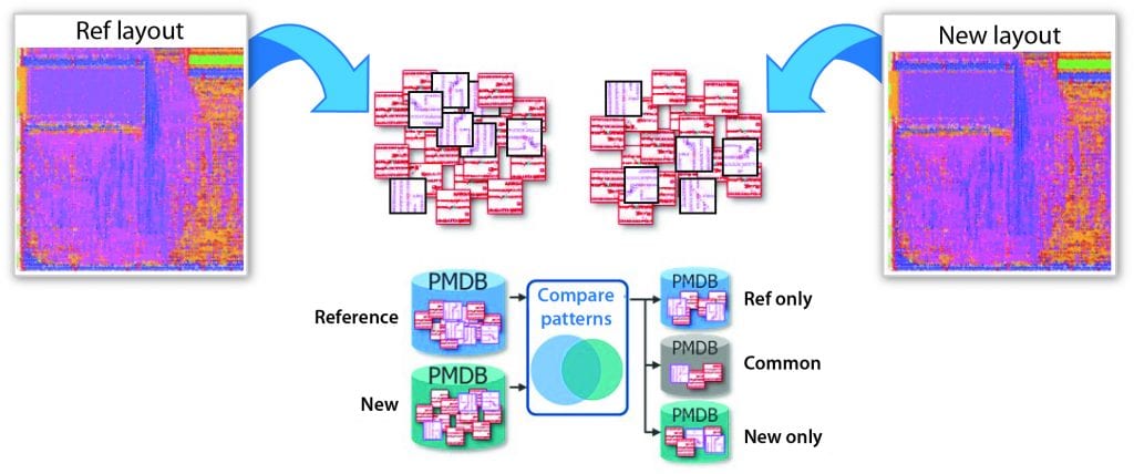
For example, in a closed-loop DFM analysis flow [4], a central/reference pattern library is used as a point of reference against a design, enabling the identification and classification of new, existing, and common information in the design when compared to the metadata stored in the reference libraries (Figure 4).

Once the reference, common, and new pattern libraries are built based on the design layout, the hotspots identified in the new design are overlaid with the reference layout for advanced debugging, failure analysis, and root cause deconvolution (RCD), as shown in Figure 5. The smart metadata reuse flow allows an extensive amount of data extraction and preparation to be reused, and enables the debugging activities to be performed in a very efficient method.

Conclusion
By preserving, inheriting, and reusing the electrical metadata generated in previous runs, a smart metadata reuse approach enables faster turnaround-time for complex geometrical checks during rechecking runs. Both runtime and resources utilization are significantly reduced, while the accuracy of the results is untouched. Debugging also benefits from the reuse of metadata, contributing to an overall reduction in TAT while ensuring and maintaining design quality. If you are looking for a more efficient and robust solution for your never-ending VLSI design and checking cycles, adopting a one-time metadata generation approach may finally allow your designers to shout “JOB DONE!”
References
1. BBC News, “Forth Bridge painting ‘is coming to an end’,” BBC.com. September 5, 2011. https://www.bbc.com/news/uk-scotland-edinburgh-east-fife-14789036
2. Sherif Hany, “Calibre PERC advanced voltage-aware DRC delivers exacting accuracy for today’s complex designs,” Mentor, a Siemens Business. Dec. 2018. https://go.mentor.com/54eVN
3. K. Kollu, F. Kharas, T. Jackson, A. Adke, “Unifying design data during verification: Implementing Logic-Driven Layout Analysis and Debug,” IEEE International Conference on IC Design and Technology (ICICDT). June, 2012. https://ieeexplore.ieee.org/document/6232874 DOI:10.1109/ICICDT.2012.6232874
4. Mentor, a Siemens business, “Samsung Foundry Closed-Loop DFM Solution Leverages Mentor Graphics Tools to Accelerate Customer Yield Ramps,” June 1, 2016.
https://www.mentor.com/products/silicon-yield/news/mentor-sumsung-closed-loop-dfm-solution
Author
Sherif Hany Mousa is a technical marketing engineer with the Design to Silicon division of Mentor, a Siemens Business, supporting Calibre physical and circuit verification products. He previously held positions as an analog quality assurance engineer and IC design consultant for physical verification and analog-mixed signal applications. Hany has several publications in the field of analog layout porting, and holds patents for an electrical-driven hotspot detection and correction flow, and advanced context-aware flow integrations. He holds a M.Sc. in electrical and communication engineering. He can be reached at sherif_hany@mentor.com.