By Emily Newton, Editor-in-Chief of Revolutionized.
Semiconductor design has progressively improved over the decades, and that will continue for the foreseeable future. Here are some fascinating trends that will likely shape the future of engineering at all stages of product development.
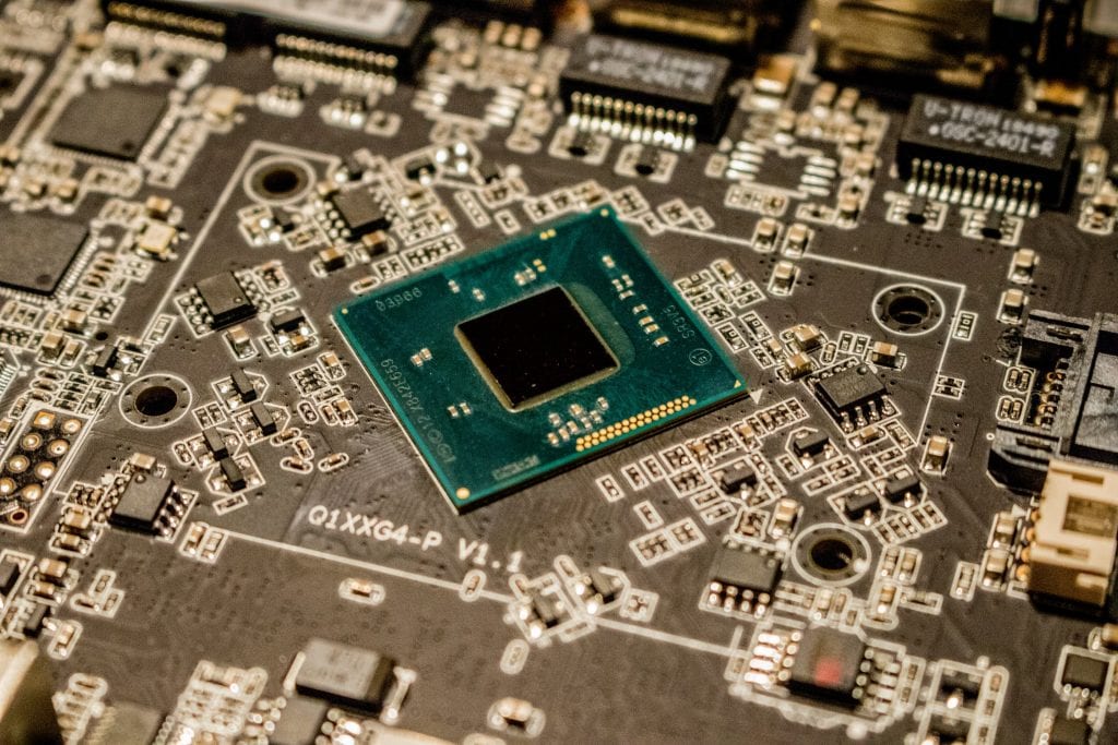
Using artificial intelligence in semiconductor design
Artificial intelligence (AI) is opening new possibilities in industries ranging from agriculture to medicine. It brings more opportunities to semiconductor design, too. Many of those should become more evident in the near future, helping engineers streamline their process and come up with pioneering products.
Analyzing magnetic properties in seconds rather than hours:
One recent example dealt with spintronics studies, which concern the intrinsic spin of electrons. Those investigations look at the limitations of silicon semiconductors’ integration levels. They apply to currently used versions, as well as efforts to develop next-generation models, such as those with ultra-low-power.
Spintronics usually requires using magnetic materials. However, it’s necessary to determine the relevant properties first, such as thermal stability and dynamic behaviors. Learning more about those parameters traditionally required engaging in time-intensive experiments. However, researchers created an AI-based system that can analyze magnetic material properties in an instant. Its estimation errors were less than 1%, making it an incredibly accurate solution.
Scientists say it used to take dozens of hours to analyze magnetic properties during semiconductor design. Now, AI can do the job in seconds.
Using AI to design more advanced future chips: One of the difficulties in designing today’s AI-powered chips is that it takes years to complete such projects. Machine learning algorithm development can happen much faster, which means some AI chips become nearly out of date as soon as they hit the market.
Engineers at Google came up with a compelling alternative. They sought to teach AI to make new chips and simultaneously shorten the design cycle.
“We have already seen that there are algorithms or neural network architectures that … don’t perform as well on existing generations of accelerators, because the accelerators were designed like two years ago, and back then, these neural nets didn’t exist,” says Azalia Mirhoseini, a senior research scientist at Google. “If we reduce the design cycle, we can bridge the gap.”
The researchers trained AI to assist with chip floorplanning. That’s a traditionally time-intensive process of deciding the placement of an integrated circuit’s major functional blocks. The goal is to minimize metrics such as power consumed and the area occupied while maximizing performance.
Results for the project showed that the deep learning reinforcement model developed for this study could produce a design in less than 24 hours. Its performance also got better with use. This led researchers to say this approach could help chip designers become more productive while also making significant improvements on existing designs.
Exploring new opportunities to keep electronics cool
Most people notice that their smartphones become slightly warm as they charge. Luckily, the warmth rarely reaches dangerous levels. That’s largely due to thermal management techniques deployed by semiconductor design experts.
Some emerging possibilities are exceptionally fascinating and could upend current cooling technologies. It will always be necessary to keep gadgets within the optimal temperature range for operating — that hasn’t changed. What has, however, are the methods selected to achieve that goal.
Pursuing liquid cooling possibilities: There has been an ongoing push for progressively smaller electronic devices. That desire in the consumer market poses additional challenges for semiconductor engineering when it comes to keeping products sufficiently cool.
However, liquid cooling options are gaining traction and will likely continue impacting design choices. Multichip packaging is a related trend. Since it involves having several chips packed into a relatively small area, heat management becomes even more challenging.
One option is to use microchannel cold plates in a semiconductor design. They distribute coolant evenly across warm surfaces. Some designs can dissipate more than 1kW/cm2 while minimizing pressure drop and surface temperature.
An industry analysis indicates that the liquid cooling sector will have approximately a $6.4 billion market worth by 2027. The coverage also mentioned semiconductors as helping drive that growth, especially since this kind of cooling offers better efficiency than air-cooled systems. However, the researchers clarified that the relatively high cost of liquid cooling could restrict its potential adoption rate.
Implementing microfluidic cooling channels into chips: Scientists recently created a new chip design that incorporates both a transistor and microfluidic cooling system into it. Engineers typically design electronic components and cooling systems separately, but this new method is a departure from that option.
One of the engineers’ goals was to eliminate the hot spots that can often develop in electronics. Professor Elison Matioli, who worked on the project, said, “We placed microfluidic channels very close to the transistor’s hot spots, with a straightforward and integrated fabrication process, so that we could extract the heat in exactly the right place and prevent it from spreading throughout the device.”
The team selected deionized water for their cooling liquid, but they’re looking at other possibilities that may be even more effective moving forward. Even if they keep using the deionized water, the team believes this approach to cooling will impact semiconductor design by leading to smaller devices that require less energy.
This achievement could also change how semiconductor engineering teams perceive the design process. In the case of this new chip, the developers knew the importance of combining electrical and mechanical engineering and thinking about cooling from the beginning instead of later. Such an approach paid off for them, and other engineers might find similar successes.
Working from home may become more common for semiconductor designers
During the COVID-19 pandemic, people specializing in semiconductor design were like many professionals from other sectors in that they had to start working from home. Their employers decided that was the safest option, especially because it helped stop the virus from spreading so rapidly.
Firsthand reports from people who shifted to that way of working often said their workplaces eventually figured out the best approaches to keep productivity high while managing distributed teams. However, they still encountered challenges.
Patrick McNamee, director of operations at EnSilica, discussed his experience during the pandemic, saying, “Daily work life at EnSilica, in common with most companies, has all moved to work from home unless absolutely necessary. For most of us, that is fine, and (the) team working by video seems not to have affected productivity too much with new designs.”
He continued, “Where we are most affected is remote debugging of test programs on (automated test equipment). This is clearly not as efficient as being there and able to just connect an oscilloscope or other instrument at will to aid with debugging.”
More recent coverage of remote working for semiconductor engineering teams emphasized how working out the challenges associated with collaboration and security became essential. Once companies did that, it became easier for them to stay on track with projects regardless of team members’ locations. Thus, now that many people are more accustomed to working remotely, it may occur more frequently even once the novel coronavirus is less of a threat.

Semiconductor design will keep evolving
As people demand more high-tech devices, semiconductor engineering will continue progressing. Whether you’re directly involved in making semiconductors or are just interested in the industry, keeping pace with new developments will put you in a great position to anticipate what the future holds for the sector. The trends listed here are some of the most notable and likely changes, but others are certainly on the horizon.


About the author: Emily Newton is a tech journalist and the Editor-in-Chief of Revolutionized.