Author’s Note: This is the last in a series of 10 installments that explore certain fundamental truths about process control—defect inspection and metrology—for the semiconductor industry. Each article introduces one of the 10 fundamental truths and highlights its implications. Within…
Samsung Foundry Begins Partnership with Silvaco to Launch their Semiconductor IP Assets
Silvaco Inc., a supplier of EDA software and design IP, announced that the semiconductor design IP of Samsung Foundry is now marketed, licensed and supported through Silvaco Inc.
Rudolph Receives First Order for its StepFAST Solution for Fan-out Panel-level Packaging
Rudolph Technologies, Inc. announced that an outsourced assembly and test facility has ordered Rudolph’s exclusive StepFAST Solution for panel-level packaging production.

Metal nanoclusters can be used as semiconductors: Key properties observed for first time
Tiny nanoclusters of metal atoms – such as gold and silver – have properties which mean they can be used as semiconductors, a joint Swansea-Hamburg research team has discovered. The finding opens the door to a wide range of potential…
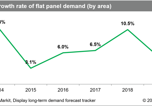
Flat Panel Display Demand Increased by Double Digits in 2018, for the First Time in Four Years
For the first time in four years, demand for flat panel displays grew double digits at 10.5 percent, year over year, to 221 million square meters in 2018.
Creating Customer Value: A Case Study on 300mm Manufacturing Learning for Back Qualification of 200mm processing
The cost of many 300mm Chemical Mechanical Planarization (CMP) consumables has decreased in recent years due to a maturing market and new process learning, making it economically feasible to embark on a new 200mm Oxide CMP polishing process based on…
Introducing Semiconductor Digest
I’m delighted to introduce Semiconductor Digest, a new business-to-business publication focused on the dynamic semiconductor manufacturing industry. Check out this link to our new Media Kit. If you’re interested in contributing content, please let me know. Our inaugural issue will…
Samsung completes 5nm EUV development
Samsung Electronics makes major strides in EUV-based advanced nodes, including 7nm mass production and 6nm customer tape-out Samsung Electronics Co., Ltd. today announced that its 5-nanometer (nm) FinFET process technology is complete in its development and is now ready for…
MagnaChip launches 28nm OLED DDIC for smartphone displays
MagnaChip Semiconductor Corporation, a designer and manufacturer of analog and mixed-signal semiconductor products, announced today that it has launched the 28-nanometer (nm) OLED (Organic Light Emitting Diodes) DDIC (Display Driver IC) for smartphone displays. The 28nm process is the most…
Semiconductor photomask sales reach record high of $4B
Following a record-breaking 2017, worldwide semiconductor photomask sales set a new high of $4.04 billion in 2018 and is forecast to extend its record-setting streak through 2020 with forecast sales of $4.2 billion, SEMI, the industry association representing the global…