Scientists at Tokyo Institute of Technology (Tokyo Tech) and Socionext Inc. have designed the world’s smallest all-digital phase-locked loop (PLL). PLLs are critical clocking circuits in virtually all digital applications, and reducing their size and improving their performance is a necessary step to enabling the development of next-generation technologies.
Wearable Medical Sensors Will Get Major Sensitivity Boost
Biosensors integrated into smartphones, smart watches, and other gadgets are about to become a reality. In a paper featured on the cover of the January issue of Sensors, researchers from the Moscow Institute of Physics and Technology describe a way to increase the sensitivity of biological detectors to the point where they can be used in mobile and wearable devices. The study was supported by the Russian Science Foundation.
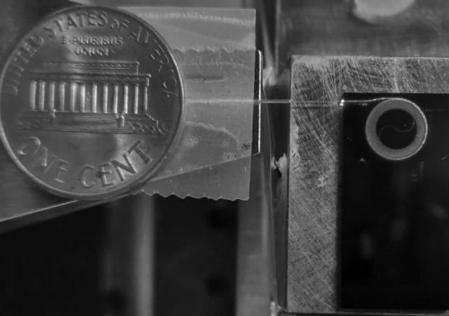
Moving Precision Communication, Metrology, Quantum Applications From Lab to Chip
The field of photonic integration — the area of photonics in which waveguides and devices are fabricated as an integrated system onto a flat wafer — is relatively young compared to electronics.
Palomar Technologies Moves to New Global Headquarters, Expands Manufacturing Footprint to Meet Growth Goals and Customer Needs
Palomar Technologies, a global leader in total process solutions for advanced photonics and microelectronic device packaging announced that to meet growing customer demand for its solutions around the world, it has moved to a new global headquarters and expanded its facilities to over 110,000 square feet.
Solid State Technology Content Now Available
The content from Solid State Technology is now available through the Semiconductor Digest website.

