Many of the most challenging optimization problems encountered in various disciplines of science and engineering, from biology and drug discovery [1] to routing and scheduling [2] can be reduced to NP-complete problems. Intuitively speaking, NP-complete problems are “hard to solve” because the number of operations that must be performed in order to find the solution grows exponentially with the problem size. The ubiquity of NP-complete problems has led to the development of dedicated hardware (such as optical annealing and quantum annealing machines like “D-Wave”) and special algorithms (heuristic algorithms like simulated annealing).

Tuning Optical Resonators Gives Researchers Control Over Transparency
Researchers at the McKelvey School of Engineering at Washington University in St. Louis have devised a fully contained optical resonator system that can be used to turn transparency on and off, allowing for a measure of control that has implications across a wide variety of applications.
EV/HEV Is Driving Power Electronics Innovations
The power electronics sector is pushing to adapt and propose innovative products. Objectives are clearly to answer to the specific needs coming from EV/HEV makers and make sure, for the power electronics companies, to be part of this attractive growth. They are so working on the miniaturization of the components, circuits and system design and are developing new solutions to integrate several systems in one system (e-axle, integration of DC-DC converter with a battery, etc.). Of course, WBG technologies are part of the technology roadmap, especially SiC power devices.
SmartSens Wins Semiconductor Solution of the Year Designation in 2020 IoT Breakthrough Awards Program
SmartSens, the leading supplier of high-performance CMOS imaging systems, today announced that its SmartSens SC132GS product has been selected as the winner of the “IoT Semiconductor Solution of the Year” award in the 4th annual IoT Breakthrough Awards program from IoT Breakthrough, a leading market intelligence organization that recognizes the top companies, technologies and products in the global Internet-of-Things (IoT) market today. As 5G and AI-enabled applications accelerate toward industry-wide ‘intelligent’ system upgrades, SmartSens’ global shutter image sensor SC132GS is built specifically to power these applications.
Picosun’s ALD Technology Enables 3D Silicon-Integrated Microcapacitors With Unprecedented Performance
Picosun Group, global provider of leading AGILE ALD® (Atomic Layer Deposition) thin film coating solutions, reports record performance of silicon-integrated, three-dimensional deep trench microcapacitors manufactured using its ALD technology. Increasing efficiency and performance demands of portable and wearable electronics, along with their shrinking size in accordance with the Moore’s law, set new challenges to the power management of these devices as well. A solution is further integration of the devices’ key components into so-called SiP (systems-in-package) or SoC (systems-on-chip) architectures, where everything, including the energy storage such as batteries or capacitors, is packed close to each other into one compact, microscale-miniaturized assembly.

China Only Region to Register Pure-Play Foundry Market Growth in 2019
IC Insights is in the process of completing its forecast and analysis of the IC industry and will present its new findings in The McClean Report 2020, which will be published later this month. Among the semiconductor industry data included in the new 400+ page report is an in-depth analysis of the IC foundry market and its suppliers.
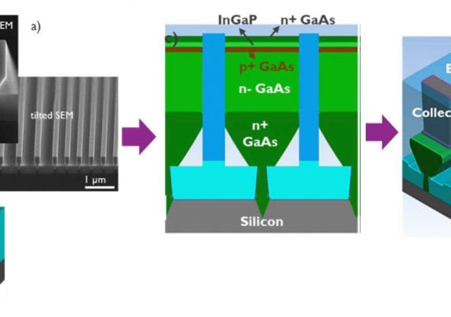
Imec Demonstrates Scalable III-V and III-N Devices on Si Targeting beyond 5G RF Front-End Modules
Imec, a world-leading research and innovation hub in nanoelectronics and digital technologies, presents the first functional GaAs-based heterojunction bipolar transistor (HBT) devices on 300mm Si, and CMOS-compatible GaN-based devices on 200mm Si for mm-wave applications.
Growing Strained Crystals Could Improve Performance of Perovskite Electronics
A new method could enable researchers to fabricate more efficient and longer lasting perovskite solar cells, LEDs and photodetectors. By growing thin perovskite films on substrates with different compositions, engineers at the University of California San Diego have invented a way of fabricating perovskite single crystals with precisely deformed, or strained, structures. Engineering a small amount of strain in perovskites is of great interest because it provides a way to make significant changes in the material’s properties, such as how it conducts electricity, absorbs and transmits light, or how stable it is.
Exact Metrology Offers $30 Challenge to Prove that the GOM CT Scanner is the Most Accurate Industrial CT Scanner on the Market
Exact Metrology, a provider of 3D and CT scanning equipment and metrology services, now offers the GOM CT scanner — the most accurate industrial CT scanner currently on the market for sale or on a contract basis. The GOM CT scanner offers the highest accuracy and highest resolution of any 225kV system available today. Additional features include a 3k detector (3008 x2512 pixels), voxel size between 2 µm – 80 µm, photogrammetric calibration, and 5-axis kinematics, measuring area of Ø 240 mm, H. 400 mm, temperature balancing and I/O port.
Inphi Surpasses Significant Milestone of 100,000 COLORZ Units Shipped
Inphi Corporation (NYSE: IPHI), a leader in high-speed data movement interconnects, today announced that it has shipped more than 100,000 COLORZ® units, the industry’s first lowest power and most cost effective 100G Silicon Photonics PAM4 platform solution for 80km DWDM connectivity in a QSFP28 form factor. The demand for bandwidth, driven by streaming video, social networking, cloud computing and mobile e-commerce, is motivating network operators to deploy cloud applications closer to the end users.