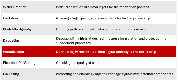
In 2024 alone, an astonishing one trillion semiconductor chips were produced – or 100 chips for every human being on earth. Behind this number is an industry racing to overcome the physical limits of semiconductors to deliver higher performance and meet soaring demand coming from the advanced AI, efficient edge computing, and premiumization in smartphone and other smart devices.
Metallization in Manufacturing & Evolution of New Materials
Today’s smart devices are performing a greater number of functions than their predecessors, particularly with the rise of AI. This has been enabled by technologies like 3D NAND in flash memory, where layers of memory are stacked vertically like skyscrapers and interconnects must be fast, precise, and defect-free.
To address higher performance requirements, one area in chip manufacturing that is undergoing transformation is metallization – the process of depositing thin metal layers on chips to form electrical pathways. Atom-by-atom deposition of metal is essential in manufacturing advanced chips — from creating complex patterns, to memory wordlines, to logic contacts.
Seven Key Stages In Semiconductor Manufacturing
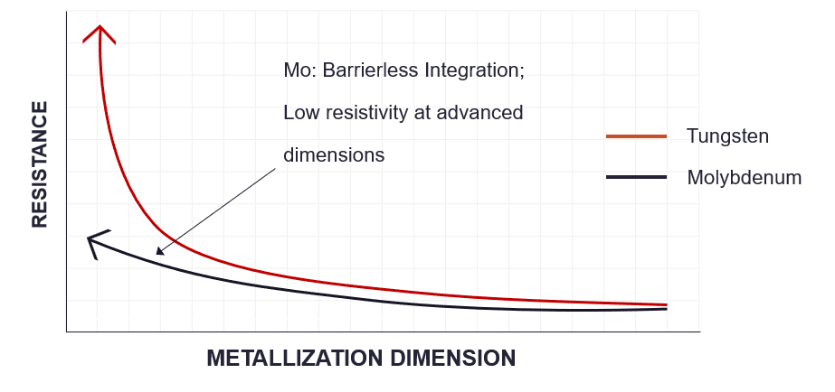
However, as layer counts increase and wordline connections – the ‘wire’ connections to memory cells – shrink, resistance and reliability become bottlenecks. This is becoming the case with Tungsten, which has been the primary element used for interconnection in the past 25 years. But as chip structures become more complex, especially with the evolution of 3D NAND and DRAM, tungsten is hitting its limits. Enter molybdenum, the metal which will propel the next leap in advanced chip manufacturing as we enter the AI era.
Why Moly, Now?
Molybdenum is superior to tungsten and offers three key breakthroughs:
- Lower resistivity than tungsten at nanoscale
- Elimination of barrier layers reducing manufacturing process steps
- Better scalability as devices shrink and layers increase
These benefits translate into faster chips, higher yields, and more efficient production—all critical for next-gen devices from smartphones to servers utilizing the three major segments across NAND, DRAM and logic chips.
Resistance Comparison
Despite its numerous benefits, molybdenum has not been used in the metallization process until now because atomic layer deposition (ALD) methods had not been developed to meet molybdenum metallization requirements. Specifically:
- Solid Precursor Delivery – The precursor, or source material, for depositing ALD molybdenum is solid in form. Hardware development is required to use and convert solid precursor to the module suitable for atomic layer deposition.
- In-Feature Deposition – Various forms of deposition are required in NAND, DRAM, and logic. Specifically, NAND requires atomic layer deposition that conformally deposits in vertical and horizontal WL structures. Logic applications can require lower temperature deposition as well as selective growth.
- Engineered Low Resistance – To achieve low resistance molybdenum, grain size and interface conditions to adjacent metal and dielectric materials is critical. Advanced ALD techniques along with hardware development are required to achieve the lowest resistance.
Cracking the Manufacturing Code For Moly:
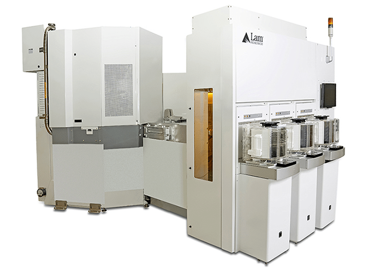
ALTUS® Halo by Lam Research – A Milestone for Molybdenum in Metallization
Lam Research’s newly launched ALTUS® Halo is the world’s first ALD tool which overcomes the technical hurdles of molybdenum deposition at scale. It delivers:
- Barrierless deposition, streamlining processes and overheads
- 50%+ reduction in word line resistance over tungsten
- Industry-leading throughput in the film growth and reduced overhead times
- Optimization across a range of metallization needs – depositing conformally or selectively
Lam Research’s ALTUS® Halo: World First Molybdenum Atomic Layer Deposition Tool
Commercial Milestones
Lam’s ALTUS Halo has made it possible to bring molybdenum into mass production. Molybdenum is now being adopted in high-volume 3D NAND and advanced logic fabs, with DRAM in development. Micron is an early adopter using ALTUS Halo in the production of its advanced NAND products.
The Bottom Line for Industry Partners and Investors
Innovation has always been a driver of value across the manufacturing chain taking the semiconductor industry forward.
“As Moore’s Law slows and semiconductor architectures become more advanced, materials innovation is the next competitive frontier,” notes Neil Shah, VP of research. “Molybdenum represents a rare and pivotal inflection point—a change not just in materials, but in terms of performance and economics of advanced chipmaking.”
Lam Research is leading this shift and delivering on innovation that will bring faster processes, better chips and more value.
Molybdenum In Semiconductor Manufacturing 101:
Download the latest whitepaper from Counterpoint and Lam Research for context around chip production processes and Molybdenum.
‘Scaling 3D Chips With Molybdenum-Based Metallization’
Watch the Counterpoint Conversations with Lam Research’s VP & GM Kaihan Ashtiani explaining the innovation around Molybdenum.
Molybdenum-Based Metallization: Unlocking New Economies of Scale in Semiconductor Manufacturing
Background
Counterpoint Technology Market Research is a global research firm specializing in products in the TMT (technology, media and telecom) industry. It services major technology and financial firms with a mix of monthly reports, customized projects and detailed analyses of the mobile and technology markets. Its key analysts are seasoned experts in the high-tech industry.