By YUDONG HAO Ph.D., Sr. Director of Marketing, Metrology Software, Onto Innovation, Milpitas, CA
Semiconductor manufacturers are increasingly challenged to measure and inspect new, smaller, and more complex 3D structures. Optical critical dimension (OCD) metrology has the fundamental capability needed for the measurements, but obtaining accurate results depends on deterministic physical modeling procedures that can be time-consuming and expensive. Artificial intelligence (AI) and machine learning (ML) techniques offer much faster solutions in many applications. Though AI and ML are unlikely to replace model-based measurements, they offer complementary strengths, suggesting that the best solutions will involve some combination of the two techniques.
What is artificial intelligence
Artificial intelligence (AI) conjures scenes from science fiction – interesting to consider but not easy to evaluate in everyday, practical terms. The term was coined in 1956 for an academic conference on the subject and used again famously by Alan Turning in a paper about the possibility of machines being able to imitate human beings doing intelligent things, such as playing chess. Since that time, AI has gone through successive cycles of favor and disfavor, as promises of great progress have fallen short on delivery. Today we may be at a tipping point, driven primarily by a tremendous expansion in the availability of data and computing power. AI is all around us. It refines results in online search and shopping. It customizes advertising and tailors news feeds. It drives cars. It designs flu vaccines. It guides, and sometimes misguides, financial markets. Most experts predict that the role AI plays in our lives will grow exponentially in almost every sector.
A brief review of concepts and terminology may be helpful. AI is not a single technology. It is better described as a collection of technologies that together allow machines to act with what looks like human intelligence. AI systems generally incorporate four fundamental capabilities: 1) the ability to sense something about the world around them with cameras, microphones or sensor of various kinds; 2) the ability to comprehend – that is, to extract information from these inputs by detecting patterns and recognizing context; 3) the ability to act based on that information; and 4) the ability to learn, refining future actions based on some evaluation of the results of past actions.
AI experts often talk about AI in terms of its strength and breadth. Weak AI appears to behave intelligently but has no real understanding of what it is doing or why. It only mimics thinking behavior. Strong AI would actually think, like a human, with a self-aware, subjective mind. Narrow AI operates within a limited set circumstances, while broad or general AI can handle a wide variety of situations, including those it has never before encountered. Finally, “superintelligence” refers to strong, general AI that exceeds human intelligence.
Machine Learning
Of the four capabilities that comprise AI, learning is perhaps the most defining. Machine learning refers to the automation of learning. It allows an AI to sense, understand, assign significance, and modify behavior in an iterative process that improves performance based on an evaluation of past results against specified criteria. Machine learning is often described in three types. Supervised learning takes data that has been organized and described (labelled), finds the salient features that characterize each category, then learns to recognize those features in new data. Unsupervised learning takes uncategorized data, finds similarities and anomalies among different entries, and categorizes them into its own groupings. Reinforcement learning works by trial and error, using a feedback loop of “rewards” and “punishments.” In reinforced learning the AI is told when its choices enhance or diminish progress toward a goal, and it tries to maximize rewards. Deep learning refers to a multi-layered learning hierarchy in which the output of each layer is the input for the next layer in the “conceptual” hierarchy. A facial recognition program might start by finding areas of light and dark, then boundaries between them, then commonalities of shapes, then noses and eyes and skin color, then distances and angles among features – all without ever knowing what a line or an eye or a color is. The interesting thing about machine learning is that it works even when we do not know exactly how it works.
Neural networks have played a key role in the in recent advances in deep learning. Neural networks are hardware or software constructs designed to emulate the function of a brain in a network of physical (electronic devices) or virtual (computer software) nodes. Neurons, the “thinking” cells of the brain, gather inputs from multiple sources and, when the inputs reach a certain threshold, send an output signal to another neuron. The relative contributions of inputs may increase or decrease based on the frequency of their occurrence or other factors, allowing a network of neurons (our brains) to recognize and reinforce recurring patterns, ultimately forming the basis of memory and cognition. Neural networks mimic this behavior and are capable of finding subtle patterns hidden in vast amounts of data.
In 1997, IBM made headlines around the world when its Deep Blue computer beat reigning world chess champion Gary Kasparov. (Kasparov reportedly claimed that Deep Blue had cheated.) Deep Blue was an example of narrow AI. It had been purpose-built to play chess and could do nothing else. By far more impressive was Google DeepMind’s AlphaGo, which became the first computer to defeat a champion at go, a complex board game popular in Asia. AlphaGo was given the rules of the game then allowed to learn by watching humans play. It learned well enough to defeat world champion, Lee Sedol. AlphaGo Zero, its successor, taught itself to win simply by playing games against itself. The next incarnation, AlphaZero, was a more general AI designed to play several games. Given the rules of the games, it taught itself to play championship chess in four hours. It also achieved championship level performance in go and shogi (a Japanese variant of chess). Some have speculated that its generalized learning capability may have contributed to its success by removing any bias against unconventional strategies. DeepMind’s latest entry in the field, MuZero was designed to learn to play games without knowing any rules. In short order, MuZero mastered chess, go, shogi, and 57 Atari games. Superintelligence? Perhaps not, but certainly extraordinary.
AI in semiconductor manufacturing
Semiconductor manufacturing is among the most complex processes ever devised. It is also among the most data-rich, with extensive records of just about anything and everything that can be measured or observed. Much of this data goes unused, at least in part because of its huge volume. Unused data is sometimes called “dark” data. AI’s ability to mine these troves of dark data for relevant relationships is one area of great promise. Other opportunities to improve process performance through the use of AI abound. They range in scale from individual process steps to the entire global supply chain and include process tool optimization, fault detection and classification (FDC), predictive tool maintenance, automatic defect classification (ADC), inspection, metrology, process control, fleet management, supply chain optimization and more. The list is practically endless. The rest of this article will focus somewhat narrowly on a specific application in optical critical dimension (OCD) metrology, as one example of the power of AI and ML.
The resolution of image based optical systems using visible light is limited by diffraction effects to about half a micrometer. The critical dimensions (CD) of semiconductor devices shrank below this limit some time ago. Optical systems were replaced by scanning electron microscopes for CD measurements (CD-SEM). As device sizes continued to shrink and dimensions of the smallest features have surpassed the measurement capabilities of CD-SEM and CD measurements had to include embedded features, manufacturers have adopted OCD, a non-image-based optical technology. OCD looks at scattering patterns in light reflected and transmitted by the measured features. When implemented on a spectroscopic ellipsometer, which captures the effects of the sample interaction with polarized light, OCD can provide fast, in-line, non-destructive characterization of the dimensions, composition, shapes, and more of complex three-dimensional features with sub-Angstrom sensitivity. Its 3D capabilities have become increasingly important for advanced devices as planar CMOS technology gives way to three-dimensional structures, including finFETs, gate-all-around (GAA) transistors, and stacked, high-aspect-ratio memory designs.
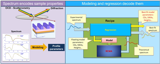
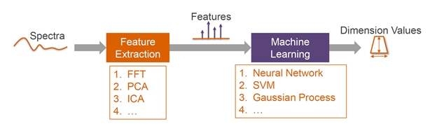
OCD is not without challenges, principal among them are time-to-solution, and requirements for massive computational power and third party reference data. OCD is an indirect measurement technique. No direct analytical solution exists to convert measurements of the optical signal directly to the physical parameters of interest. Rather, the analysis requires computationally intensive modeling of the expected pattern based on physical calculations and regression analysis of a large number of spectra (FIGURE 1). The measured spectrum is then compared to the modeled spectra to find the best fit, from which the parameters of interest are inferred. Here lies the opportunity for artificial intelligence. Given an appropriate data set and using machine learning, AI can find the salient spectral features and quantify their relationships to the parameters of interest without physical modeling or structured regression analysis (FIGURE 2).


AI solutions for OCD are unlikely to replace model-based solutions, rather they will provide complementary capability in situations where modeling is especially challenging. For simple, familiar structures, where modeling is uncomplicated, model-based analysis will continue to be the method of choice. The major challenge of ML-based OCD comes when the often-limited labeled data set unable to uncover the complicated nonlinear relationship between the optical signal and multiple dimensions. This situation leads to over-learning, a common pitfall in ML that gives “good” prediction only within the provided data set but would fail to predict unknown data in a so-called blind test. More reference data will improve ML performance, but the extra cost and delay to get more reference data from an oftentimes destructive method can quickly negate the benefit of ML-based solutions. As a result, the ideal space for AI solutions will be situations where 1) modeling costs are high because the structure is complex, non-periodic, or has a high 3D pitch; 2) the key parameter of interest has a dominating or unique sensitivity in the signal (such as dielectric CMP or DRAM overlay and 3D NAND channel hole tilt measurements showcased in the next sections); and 3) extensive reference data is available from CD-SEM and cross sectional SEM, well-designed experiments (DOE), or multiple process knobs.
Use cases for machine learning solutions in OCD metrology
Spectroscopic ellipsometry (FIGURE 3) looks at changes in polarized light when it is reflected/transmitted by features and layers of the sample, specifically it measures changes in amplitude and phase (retardance) of the s and p components of the polarized beam. These changes can be completely described mathematically using Mueller calculus in which the light is characterized by a 4-dimensional Stokes vector, and the optical elements with which it interacts by 4×4 Mueller matrices. Single compensator ellipsometers can acquire up to twelve of the sixteen components of the matrix. Only dual rotating compensators can resolve all 16 independent Mueller channels. The four matrix components that complete the Mueller Matrix ensure the integrity of full Mueller Matrix, which is particularly critical for measuring structural asymmetry. The off-diagonal components of the matrix are uniquely sensitive to parameters like tilt and overlay that violate structural symmetry. In order to achieve the highest quality signal, a proprietary compensator is used to provide consistently high sensitivity across the entire UV-IR wavelength range, while the common waveplate compensators show large wavelength-related changes in retardance sensitivity in the UV-visible range and low sensitivity in IR.
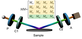
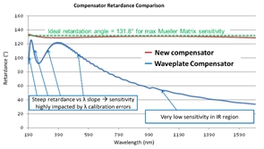
Figure 3. Acquisition of a full Mueller Matrix requires dual rotating compensators to deliver constant, high sensitivity over the entire UV-IR wavelength range.
Mueller Matrix measurement of on product overlay for DRAM
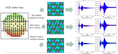
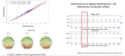
Mueller Matrix’s unique sensitivity enables measuring after-etch overlay in DRAM directly on device with the help of machine learning. FIGURE 4 shows full wafer data from a DOE sample with programmed overlay variation across the wafer designed cover expected process variation of DRAM on product overlay. The figure includes magnified top-down view illustrations of the overlay errors between Word Lines (horizontal green bars) and the STI islands (slanted rounded rectangles), negative toward the top region, zero in the middle and positive toward the bottom; and the corresponding Mueller Matrix asymmetry signals. FIGURE 5 plots training data and test measurements, showing strong correlations (R2 better than 0.95 for both) and similar slopes. In order to test the robustness of this result, we systematically reduced the number of reference data for training from the total set to check the prediction performance. The plots on the right show that stable performance was achieved for both R2 and slope measurements after only 36 references from three sister wafers. That means four points from each of the three DOE regions are sufficient to predict over the whole wafer.


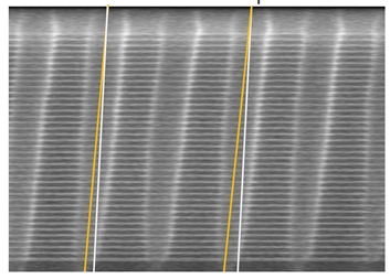
Tilt measurements in high aspect ratio etch
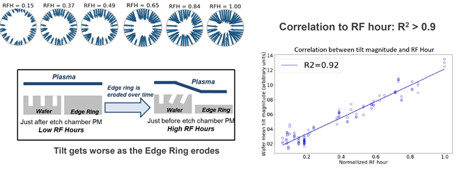
3D NAND uses high aspect ratio channels (FIGURE 6) created with reactive ion etch (RIE). The channels ultimately become vertical stacks of memory cells. RIE systems use a focus ring to maintain continuity in the plasma sheath near the edge of the wafer and ensure good etch uniformity. The focus ring erodes over time during the etch process, changing its height and shape and causing the channel etch profiles to tilt off-vertical, which can be uniquely picked up by the Mueller Matrix off-diagonal signal. FIGURE 7 shows tilt measurements made with machine-learned Mueller Matrix spectroscopic ellipsometry. The radial vectors in the wafer plots across the top of the figure show the tilt increasing over RF hours, basically how long the focus ring has been bombarded by etchants. The plot to the right shows strong correlation (R2=0.92) between RF hours and tilt magnitude.


Logic SRAM
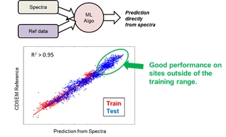
In the final example (FIGURE 8), CD measurements on logic SRAM, the system was trained directly on CD-SEM reference data. There was no structure modeling and all measurements were made on-device. Time-to-solution was much faster than modeling. The measurements showed good correlation (R2 > 0.95) for both training and test data, which extended to test points outside the training range.

Summary
Artificial intelligence has become an important tool for optimizing system and process performance in a wide variety of industrial and commercial applications. Machine learning allows AI to self-optimize, without understanding the cause and effect relationships of the correlations it discovers. Together, AI and ML have great potential in many areas of the semiconductor manufacturing process, ranging in scale from improving the performance of individual tools to managing an entire fab and optimizing the global supply chain. Specific examples here have shown AI/ML solutions for OCD measurements that avoid the lengthy and costly modeling process required by conventional solutions. Though unlikely to replace model-based solutions, machine learning solutions will provide complementary capability in complex, time sensitive situations where the cost and time required for modeling is prohibitive. Applications of AI/ML in other areas of the semiconductor industry are likely to grow rapidly as manufacturers discover the value hidden in their data.
Acknowledgements
The author would like to acknowledge and thank SK hynix, Micron and Peilin Ong, Guat Beng Chu, Luey Chwan Liong, Jeffery Woo, Zhuan Liu, Shilin Ng, Saurabh Singh, Padraig Murphy and Kevin Heidrich for their contributions to this work. The views expressed here are the author’s alone.
References
1. Shilin Ng, High Aspect Ratio Etch Tilt Detection with Full 4×4 Mueller Matrix Spectroscopic Ellipsometry and Its Application to 3DNAND Channel Hole Etch Process and Chamber Monitoring, AVS 65th International Symposium & Exhibition