Researchers in UC Santa Barbara/Google scientist John Martinis’ group have made good on their claim to quantum supremacy. Using 53 entangled quantum bits (“qubits”), their Sycamore computer has taken on — and solved — a problem considered intractable for classical computers. The milestone comes after roughly two decades of quantum computing research conducted by Martinis and his group, from the development of a single superconducting qubit to systems including architectures of 72 and, with Sycamore, 54 qubits (one didn’t perform) that take advantage of the both awe-inspiring and bizarre properties of quantum mechanics.
Packaging
Combination of Nanometrics and Rudolph Technologies to Create Onto Innovation
Nanometrics Incorporated (NASDAQ: NANO) and Rudolph Technologies, Inc. (NYSE: RTEC), today announced that their combined company will be named Onto Innovation Inc., following the close of their previously announced merger of equals. The name Onto Innovation reflects the combined company’s anticipated focus on the future and exciting challenges ahead, highlighting the increasing importance of innovation in enabling that future for the company and its broader served markets. Onto Innovation will bring a breadth of perspective across the entire semiconductor value chain to innovate and enable its customers to solve their most difficult yield, device performance, quality, and reliability issues.
NSITEXE Achieves First-Pass Silicon Success for High-Performance Data Flow Processor-based SoC Test Chip Using DesignWare IP
Synopsys, Inc. (Nasdaq: SNPS) today announced that NSITEXE, a Denso Group Company, achieved first-pass silicon success for its high-performance Data Flow Processor (DFP)-based SoC test chip using Synopsys’ DesignWare® Interface and Foundation IP portfolios. With Synopsys’ silicon-proven DesignWare IP, NSITEXE met the advanced functionality, processing, performance, and testability requirements of its DFP-based SoC. NSITEXE’s DFP-based SoC combines both a CPU and a GPU to process large and complex datasets for parallel data management with power-efficient parallelism and quality.
OneSpin Shows How to Achieve IC Integrity at DVCon Europe
OneSpin® Solutions, provider of certified IC integrity verification solutions for building functionally correct, safe, secure and trusted integrated circuits, will present its verification expertise through a tutorial, technical session and an exhibit at DVCon Europe, being held October 29 – 30, 2019 at the Holiday Inn Munich City Centre, Munich, Germany.
Renesas Expands Access to Portfolio of Leading-Edge IP Licenses
Renesas Electronics Corporation (TSE:6723), a supplier of advanced semiconductor solutions, today announced expanded access to its highly sought portfolio of intellectual property (IP) licenses that allow designers to meet a broad range of customer requirements in a rapidly changing industry. Starting today, customers will have access to IPs such as advanced 7nm (nanometer) SRAM and TCAM, and leading-edge standard Ethernet time-sensitive networking (TSN) IP. Furthermore, Renesas is working on providing a system IP which includes PIM (processing in memory), which attracted attention as an AI accelerator, presented in a conference paper in June 2019.
Micron Brings 3D XPoint Technology to Market With the World’s Fastest SSD
Micron Technology, Inc. (Nasdaq: MU), today announced a breakthrough in nonvolatile memory technology with the introduction of the world’s fastest SSD, the Micron X100 SSD. The Micron X100 SSD is the first solution in a family of products from Micron targeting storage- and memory-intensive applications for the data center. These solutions will leverage the strengths of 3D XPoint technology and usher in a new tier in the memory-to-storage hierarchy with higher capacity and persistence than DRAM, along with higher endurance and performance than NAND.
StratEdge Offers Assembly Services for Die Attachment on CMC Tabs
StratEdge Corporation announced its assembly services for attaching gallium nitride (GaN) and other high-frequency, high-power devices using gold-tin (AuSn) and gold-silicon (AuSi) onto copper-molybdenum-copper (CMC) tabs. StratEdge’s proprietary eutectic die attach method maximizes the power output a chip can achieve, optimizing its performance and providing an efficient way to dissipate heat to avoid overheating and failures during normal operation.
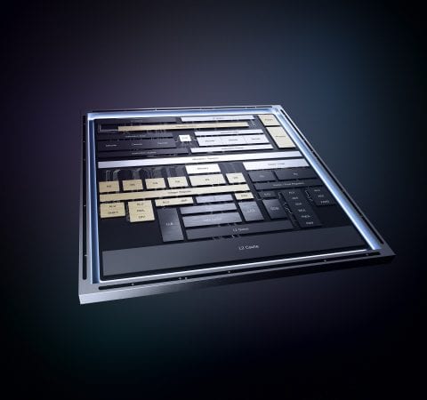
Intel Introduces Tremont Microarchitecture
Today at the Linley Fall Processor Conference in Santa Clara, Calif., Intel revealed the first architectural details related to Tremont. Intel’s newest and most advanced low-power x86 CPU architecture, Tremont offers a significant performance boost over prior generations.
ASE Group Significantly Advances Semiconductor Packaging Development With ANSYS Customization Toolkit Solution
ASE Group (ASE) engineers have drastically improved their integrated circuit (IC) semiconductor packaging and development process to create state-of-the-art microchips thanks to ANSYS (NASDAQ: ANSS). Developing an ANSYS Customization Toolkit (ACT) solution, engineers create more accurate models, enhance structural reliability and slash design time to enable customers to receive products faster than ever.
North American Semiconductor Equipment Industry Posts September 2019 Billings
North America-based manufacturers of semiconductor equipment posted $1.95 billion in billings worldwide in September 2019 (three-month average basis), according to the September Equipment Market Data Subscription (EMDS) Billings Report published today by SEMI. The billings figure is 2.4 percent lower than the final August 2019 level of $2.00 billion, and is 6.0 percent lower than the September 2018 billings level of $2.08 billion. “Monthly billings of North American equipment manufacturers declined for the second consecutive month,” said Ajit Manocha, president and CEO of SEMI.