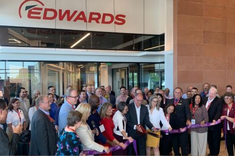
Edwards has significantly expanded in the U.S. in recent years, with a new 200,000 ft2 facility in Chandler, AZ, a state-of-the-art chemical laboratory at its Innovation Center in Hillsboro, OR and, most recently, new plans for a new dry pump manufacturing facility in Genesee County, NY.
Packaging
Changes Coming to the CIS Ecosystem
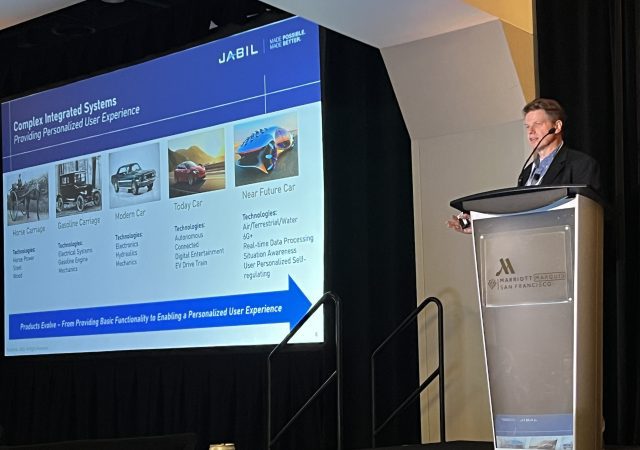
Speaking at the Market Symposium at SEMICON West on Monday, Dan Gamota, Vice President, Manufacturing, Innovation & Product Industrialization, Jabil, described a changing landscape for the electronics manufacturing ecosystem, where the lines between chip-makers, foundries, electronics manufacturing service (EMS) providers and OSATS (outsourced assembly and test services) are blurring.
Marposs Acquires Solarius and Strengthens Its Semiconductor and Consumer Electronics Segment
The Silicon Valley based company Solarius becomes part of the Marposs Group, strengthening the technology of the Italian multinational company in the semiconductor industry.
Arizona State University and Applied Materials to Create “Materials-to-Fab” Center
More than $270 million in corporate and state investment will help advance Arizona’s semiconductor industry.
Global Semiconductor Equipment Sales Forecast: $87 Billion in 2023 With 2024 Rebound, SEMI Reports
Global sales of total semiconductor manufacturing equipment by original equipment manufacturers next year are forecast to bounce back from a projected contraction of 18.6% to $87.4 billion in 2023 following the industry record of $107.4 billion in 2022.
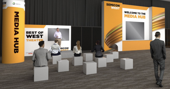
SEMI and Semiconductor Digest Announce 2023 Best of West Award Finalists
SEMI and Semiconductor Digest today announced finalists for the Best of West award to be presented at SEMICON West 2023, July 11-13 at the Moscone Center in San Francisco.
SEMICON West 2023 Opens Tomorrow to Showcase Industry Growth to $1 Trillion, Sustainability and Talent
Concurrent with SEMICON West, FLEX Conference 2023 to Spotlight Flexible Hybrid Electronics Innovations.
Applied Materials Advances Heterogeneous Chip Integration with New Technologies for Hybrid Bonding and Through-Silicon Vias
Applied Materials, Inc. today introduced materials, technologies and systems that help chipmakers integrate chiplets into advanced 2.5D and 3D packages using hybrid bonding and through-silicon vias (TSVs). The new solutions extend Applied’s industry-leading breadth of technologies for heterogeneous integration (HI).
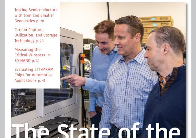
What’s in the July Issue?
Each issue of Semiconductor Digest has articles found only in the magazine. Click on the links to read the articles in the July issue. Pick up your copy in print at SEMICON West in the publication bins and at the Semiconductor Digest Booth 1829.
ChipFlow Raises £1.2M in Pre-Seed Funding to Democratize Semiconductor Design Through Open-Source Software Tools
The oversubscribed financing round, which was led by Fontinalis Partners, includes participation from Fuel Ventures, InMotion Ventures, the investment arm of JLR, APX, and others.