Diodes Incorporated introduces the latest addition to its portfolio of Silicon Carbide (SiC) products: the DMWS120H100SM4 N-channel SiC MOSFET.
Packaging
U.S. Secretary of Commerce Gina Raimondo Announces Fiber Manufacturing Expansions in North Carolina
Today, as part of the Biden-Harris Administration’s Investing in America tour, U.S. Secretary of Commerce Gina Raimondo and Assistant Secretary of Commerce for Communications and Information Alan Davidson traveled to Hickory, NC to celebrate the announcement of new fiber optic cable production in the U.S. made possible by the Administration’s Internet for All Initiative.
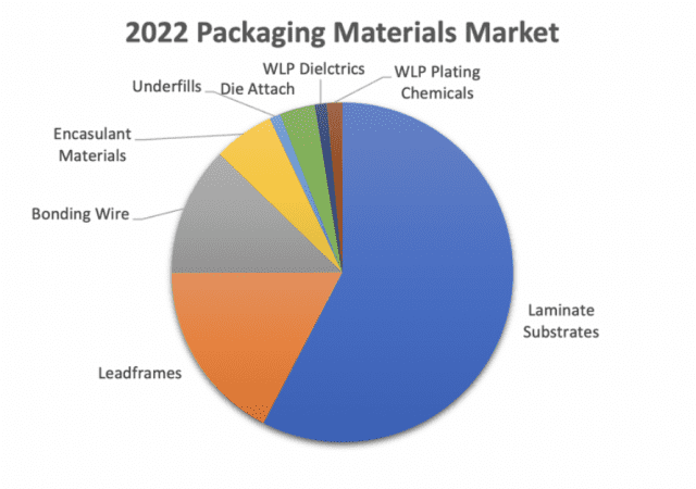
New Global Semiconductor Packaging Materials Outlook – US$26B Market to Approach US$30B by 2027
TECHCET and TechSearch International, Inc. recently announced that the market for Semiconductor Packaging Materials totaled US$26.1 billion in revenues for 2022, and is forecasted to approach US$30 billion in 2027.
New SIA Map Highlights Broad U.S. Semiconductor Ecosystem
The semiconductor ecosystem in the United States is broad and diverse, as illustrated by SIA’s new U.S. Semiconductor Ecosystem Map, a first-of-its-kind tool that allows users to explore industry activities across the country, including nearly 500 locations in 42 states.
New Chip Design to Provide Greatest Precision in Memory to Date
A team led by USC, MIT, and the University of Massachusetts, developed a protocol for devices to reduce “noise” and demonstrated the practicality of using this protocol in integrated chips.
ACM Research Receives First Purchase Order for Ultra C SiC Substrate Cleaning Tool
The platform leverages ACM’s patented Space Alternated Phase Shift (SAPS) cleaning technology which is designed to achieve more comprehensive cleaning without damage to device features.
Adeia Signs Long-Term Semiconductor Patent License Agreement with Kioxia
Adeia Inc., the company whose patented innovations enhance billions of devices, today announced that Kioxia Corporation entered into a long-term agreement to license Adeia’s semiconductor patent portfolio, including those relating to hybrid bonding.
Pfeiffer Vacuum Offers a New Vacuum Calculator
Pfeiffer Vacuum offers their customers a vacuum calculation tool to identify specific vacuum products for their application, examine evacuation as well as pump down curves and perform different calculations for self-configurated pumping solutions.
New Resources for CHIPS Applicants
Today, the Department of Commerce is releasing pre-application and application instructions, guidebooks, and other resources for the first CHIPS for America funding opportunity for leading-edge, current-generation, mature-node, and back-end semiconductor fabrication facilities.
Park Systems Introduces Park NANOstandard for Traceable Calibration Standards
Park Systems, a provider of Atomic Force Microscopy (AFM) and nano-metrology solutions, announced the launch of its Park NANOstandard product line.