Last November AMD held their AMD Accelerated Data Center Premiere, Intel had their Innovation Days, and Stephen Shankland of CNET visited Intel’s fabs 42 and CH-4 in Chandler.
Siliconica
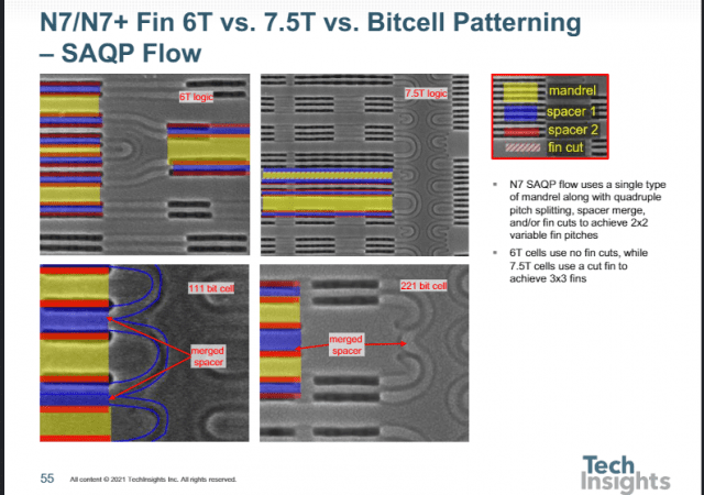
Comprehensive Report on FinFET Front-End Evolution Just Released by TechInsights
In the field of reverse engineering, TechInsights is the world’s leading provider of analyses of advanced technology and associated intellectual property services to many of the world’s most successful technology companies.
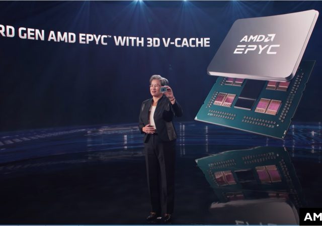
AMD Announces Use of TSMC 3D Fabric for Stacked Vertical SRAM Cache, TechInsights Confirms Current Ryzen 5950X is TSV-Capable
At Computex a couple of months ago Lisa Su of AMD gave a keynote talk detailing their new products, but at the tail end she surprised attendees by discussing their advancements in packaging technology.
A Claim That TSMC Has a 1nm Process Hits the Headlines
Less than two weeks after IBM announced their 2-nanometer CMOS technology, UK website Verdict picked up on a paper published in Nature and somehow morphed that into a claim that TSMC had made breakthrough in 1-nm technology development.
IBM Announces 2nm GAA-FET Technology – the Sum of “Aha!” Moments
IBM likes to create a stir once in awhile, and judging by the tech-press response in the last week or three, they have achieved that goal with their announcement of 2-nanometer CMOS technology, developed at their Albany research centre. This technology is expected to give a 45% performance boost or 75% power reduction, compared with a 7-nm process. Of course the question is, compared with what 7-nm process?
Gate-All-Around Transistors Show up at ISSCC
The International Solid-State Circuits Conference was held virtually last month from February 13th – 22nd, 205 papers in 35 sessions, with industrial participation from Analog Devices, Broadcom, Huawei Technologies, IBM, Intel, Qualcomm, Realtek Semiconductor, Renesas, Samsung, Sony, SK Hynix, STMicroelectronics, TSMC, Texas Instruments, and more.
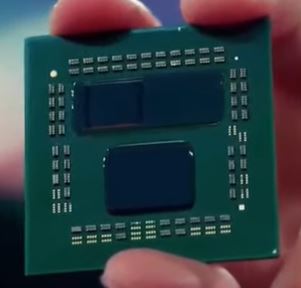
ICYMI – Intel Shows Early Ponte Vecchio Part
Occasionally, we will see something in the media that we think worth commenting on, and post as an “In Case You Missed It” (ICYMI) blog. In this case, it was a Jan 26 Twitter post by Intel’s Raja Koduri (@rajaonthe edge), showing a complex multi-die part that appears to be the Ponte Vecchio high-end GPU, announced by Raja in his keynote at the Intel HPC Developer Conference just before SuperComputing 2019.
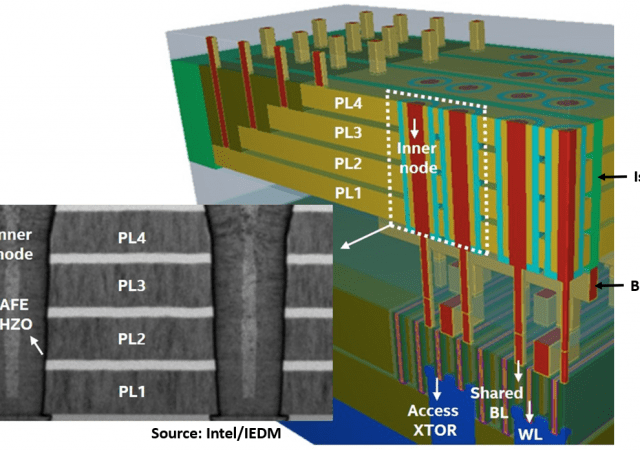
Intel Looks Ahead to Stacked Nano-Ribbon Transistors, Anti-Ferroelectric E-DRAM at IEDM
Thanks to Covid-19, IEDM goes virtual this year, over the weeks of December 5 – 18th. After scanning through the advance program, and the tipsheet, a couple of papers from Intel caught my eye, one on complementary stacked nanoribbon transistors, and the other detailing embedded DRAM using anti-ferroelectric (AFE) capacitors.
Intel Replaces 10+ with Tweaked SuperFin Technology
Intel held their virtual 2020 Architecture Day on August 13th, hosted by Raja Koduri, and the first major topic was Process Innovations, with Ruth Brain as the presenter. Ruth started with a potted history of Intel processing, from the first strained channel at the 90-nm node to the string of 14-nm evolutions.
Update: TSMC’s 5nm CMOS Technology Platform
At the International Electron Devices Meeting (IEDM) in San Francisco December 7-11, Geoffrey Yeap presented the talk “5nm CMOS Production Technology Platform Featuring Full-Fledged EUV and High-Mobility Channel FinFETs with Densest 0.021µm2 SRAM Cells for Mobile SoC and High-Performance Computing Applications”. Contributing Editor Dick James provides an update on his original pre-IEDM blog.