Samsung gives a second paper this session, detailing (2.5) A Novel Integration of STT-MRAM for On-chip Hybrid Memory by Utilizing Non-Volatility Modulation, with Jeong-Heon Park as lead author. “We demonstrate a novel way of integrating STT-MRAM for on-chip hybrid memory which exhibits either features of high-retention or high-speed implemented in separate zones in a single chip. For satisfying high temperature retention requirement, tailored MTJs are shown to support >10-year retention at 220℃.” MRAM switching protocols can be tuned for either high speed or high retention, so here we have a process which gives the option of both on the same die.
Siliconica
IEDM’s Monday is MRAM Day
Session 2 (Memory Technology – STT-MRAM) on Monday afternoon at IEDM has a series of industrially-based papers, starting with Everspin, one of the few commercial producers of MRAM; Demonstration of a Reliable 1 Gb Standalone Spin-Transfer Torque MRAM For Industrial Applications, Sanjeev Aggarwal et. al, Everspin Technologies.
Intel Updates Advanced Packaging Technologies at SEMICON West Part 3
The SEMICON West workshop was unusual in that all the presenters were from Intel’s Assembly Test Technology Development (ATTD) group, and the session kicked off with a review of ATTD by Corporate VP Babak Sabi. The scope of their activities ranges from wafer sort, die preparation, and identifying known good die, through assembly, test, die finish, and board development, and also substrates, tooling, and other assembly materials; so pretty well the whole spectrum. They have quite the complex in Chandler (Arizona), as well as other facilities in Oregon and Malaysia.
Intel Updates Advanced Packaging Technologies at SEMICON West Part 2
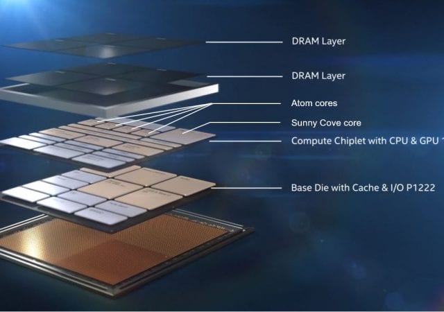
At the Architecture Day Intel demoed a Foveros-based part, comprising a high-performance 10-nm chiplet on a low-power 22nm base die. The upper die contained five cores, four Atom low-power cores and a high-performance core, and as shown in the Intel image above, the two lower dies were stacked with PoP memory, all in a 12 x 12 mm package with 2mW standby power.
Intel Updates Advanced Packaging Technologies at Semicon West, the Latest in a Decade (or more) Evolution
In the last several years, Intel has had a series of announcements in the packaging arena, focused on the integration of multiple styles of chips in the same package to improve performance and broaden system capabilities.
The Second Shoe Drops – Now We Have the Samsung V-NAND Flash
By Dick James, Senior Technology Analyst, Chipworks Two weeks ago, we posted about the TSMC…
The Second Shoe Drops – Now We Have the Samsung V-NAND Flash
By Dick James, Senior Technology Analyst, Chipworks Two weeks ago, we posted about the TSMC…
TSMC 20nm Arrives – The First Shoe Drops
By Dick James, Senior Technology Analyst, Chipworks For us at Chipworks interested in leading edge…
TSMC 20nm Arrives – The First Shoe Drops
By Dick James, Senior Technology Analyst, Chipworks For us at Chipworks interested in leading edge…
Intel’s e-DRAM Shows Up In The Wild
When Intel launched their Haswell series chips last June, they stated that the high-end systems…