JAY ZHANG, Corning Incorporated, CHEE-HAU NG, United Microelectronics and SEBASTIEN KOUASSI, pSemi
The RF world has been taken by storm with innovative materials in the last 10 years. This surge of innovation has been an important factor in bringing mainstream high data transfer speeds enabling 3G, 4G and now 5G protocols. Need for more and more frequency bands, and higher speeds for 5G/6G enabled by carrier aggregation drive the need for better harmonics control in RF front-end (RFFE) ICs. Moving the substrate of RFFE ICs towards a pure dielectric material is one possible solution. Among candidate dielectric materials, glass offers not only attractive material properties such as tailorable coefficient of thermal expansion (CTE), low dielectric loss and low nonlinearity, it is also scalable to 300mm wafer size to be able to leverage advanced node technologies.
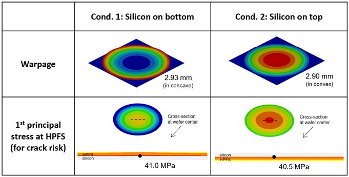
However, glass is a “foreign” material for CMOS foundries as it brings the risk of contamination alongside its implementation. The benefit of glass in RF has already been demonstrated with integrated passive devices on glass [2], but there is a higher barrier to build active devices on glass. The benefits nevertheless can be very important and differentiating. Indeed, glass is the best candidate one can imagine using to build RF devices. This is because it is virtually transparent to the RF devices fabricated on top of it as the resistivity and dielectric constant beat any other existing materials in the Si family. It is in particular a better candidate than the current state of the art material RFSOI, and the glass wafer ecosystem is ready supply wafers in the desired quantities.

UMC’s good experience in wafer-to-wafer bonding, Corning’s competency in glass wafer engineering and manufacturing, and pSemi’s expertise in RF devices using breakthrough technologies formed the basis of a natural consortium to tackle the associated challenges. In this article, published in the December 2021 issue of Semiconductor Digest, the authors detail the challenges and successes they encountered evaluating 300mm glass wafer material in a production foundry environment.