Extreme Ultraviolet Lithography (EUV) has emerged as the technology of choice for patterning the most critical dimensions for the 7 nm node and beyond. However, resist pattern collapse is one of the hurdles that is preventing a comfortable process margin/window for resist patterning. One approach to suppress this pattern collapse is to use a rinse step after the DI water rinse that typically followed resist development, and before the final dry out.
In a recent set of experiments, new rinse materials developed by the Electronics business of Merck KGaA, Darmstadt, Germany which operates as EMD Electronics in the U.S. and
Canada, have proven to be effective in defect reduction, especially defects
related to resist residue. The work was presented by Kazuma Yamamoto,
Manager of EUV Ancillaries at EMD Electronics, at SEMI Strategic Materials
Conference in Korea.
As shown in Figure 1, pattern collapse is caused by the capillary force between resist patterns during rinsing and drying in the development process. The main factors of capillary force are the surface tension and the contact angle of the rinsing liquid and also the pattern structure (line width, space width, and height). The collapse will occur when the tensile stress a caused by the rinsing liquid exceeds the adhesion force between photoresist patterns and the substrate.

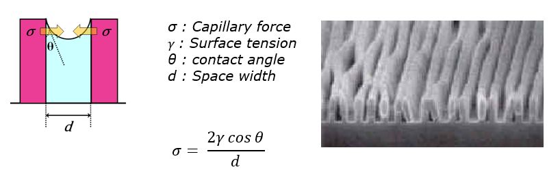
“The prevalent develop processes for chemically amplified resists are water/TMAH-based,” explained Jeff Catlin, Head of Business Field, Patterning Solutions at EMD Electronics. “To stop or quench the reaction of the developer, you do a DI water rinse.” This is followed by a high-speed spin to cast all the water off the wafer. “As the water dries, the meniscus between adjacent two photoresist lines creates surface tension strong enough to pull the lines together,” he said.
Although the exact formulation is proprietary, the new rinse material developed by EMD Electronics, includes a surfactant that lowers surface tension to mitigate pattern collapse, and also controls affinity to the resist to prevent pattern bridging. The step is performed prior to the high-speed spin.
Read the full article in the April/May issue of Semiconductor Digest.