The Northeast Microelectronics Coalition (NEMC) Hub, a division of the Massachusetts Technology Collaborative (MassTech) launched the SCALE Capital program, a $10 million grant initiative to advance microelectronics capability, training and product development across Massachusetts.
Veeco’s WaferStorm and WaferEtch Wet Processing Platforms Qualified for Advanced Packaging Applications
Veeco Instruments Inc. today announced a global Semiconductor IDM qualified Veeco’s WaferStorm and WaferEtch platform for two new applications in Advanced Packaging.
HKUST Research Sheds Light on Future Applications in Spintronics and Valleytronics
A team led by Prof. LIU Junwei from the Department of Physics at the Hong Kong University of Science and Technology (HKUST), along with their experimental collaborators, published their latest research findings in Nature Physics, which unveiled the first experimental observation of a two-dimensional layered room-temperature altermagnet, validating the theoretical predictions in Nature Communications made by Prof. Liu in 2021.
DNA-Inspired Design for Stronger, Flexible Sensors for Wearables
The double-helical design places both electrodes at one end, preventing damage that typically occurs when electrodes are pulled at joints.
Seoul Semiconductor: Unified Patent Court Orders Recall of Products Infringing Essential Micro LED Patents
Seoul Semiconductor Co., Ltd., a global innovator of LED products and technology, announced that the Local Division Paris of the Unified Patent Court (UPC), which has jurisdiction across 18 European countries, has issued a judgment that Laser Components SAS infringed Seoul Semiconductor affiliate’s core optical semiconductor patent.
Researchers Develop a Novel Annealing Processing System
In a groundbreaking study, a research team from Japan, led by Professor Takayuki Kawahara from the Department of Electrical Engineering at Tokyo University of Science, Japan, developed an innovative dual scalable annealing processing system (DSAPS) that can simultaneously scale both capacity and precision using the same scalable structure.
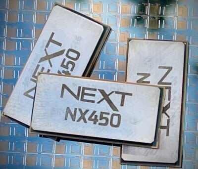
NEXT Semiconductor Technologies Collaborates with BAE Systems to Develop Next Generation Space-Qualified Chips
NEXT Semiconductor Technologies is collaborating with BAE Systems to accelerate the insertion of its latest ultra-wideband antenna processor units (APUs) into high-performing radiation-hardened electronic subsystems to support future space missions.

2024 Global Semiconductor Materials Market Posts $67.5 Billion in Revenue, SEMI Reports
Global semiconductor materials market revenue increased 3.8% to $67.5 billion in 2024, SEMI, the global industry association representing the electronics design and manufacturing supply chain, reported today in its Materials Market Data Subscription (MMDS).
Advanced Semiconductor Packaging Market Forecast to Grow at 7.5% CAGR Through 2031
The Advanced Semiconductor Packaging Market was valued at USD 18090 Million in the year 2024 and is projected to reach a revised size of USD 29800 Million by 2031, growing at a CAGR of 7.5% during the forecast period.
OKI Develops 124-Layer PCB Technology for Next-Generation AI Semiconductor Testing Equipment
OKI Circuit Technology has successfully developed 124-layer PCB technology for wafer inspection equipment designed for next-generation high bandwidth memory, such as HBM mounted on AI semiconductors.