Advanced, smart and green manufacturing will take center stage on-site and online September 23-25 as SEMICON Taiwan 2020 gathers industry visionaries and experts for the latest market trends, business opportunities and innovations across the semiconductor supply chain.
ClassOne’s Solstice LT Plating System Selected by Jenoptik for Producing High-Power Diode Lasers
Semiconductor equipment manufacturer ClassOne Technology announced the sale of its Solstice LT electroplating system to Jenoptik for manufacturing semiconductor material for high-power diode lasers at its semiconductor production facility in Berlin-Adlershof, Germany.
Fan-Out Wafer Level Packaging for next Generation mmWave Antenna in Package Applications
A*STAR’s Institute of Microelectronics (IME) has collaborated with leading industry players to establish 300mm Wafer Level Package development line (WLP-DL) to drive the application of fan-out wafer level packaging (FOWLP) for achieving innovations in current and next generation system-in-package (SiP).
Second Quarter 2020 Global Semiconductor Equipment Billings Up 26% Year-Over-Year, SEMI Reports
Second quarter 2020 global billings for semiconductor manufacturing equipment jumped 26% year-over-year and 8%, to US$16.8 billion, from the first quarter of the year, SEMI announced today in its Worldwide Semiconductor Equipment Market Statistics (WWSEMS) Report.
Imec and Ghent University Present a Smart Contact Lens Mimicking the Human Iris to Combat Eye Deficiencies
Imec, a world-leading research and innovation hub in nanoelectronics and digital technologies and CMST (an imec-affiliated research group at Ghent University), together with their partners the Instituto de Investigación Sanitaria Fundación Jiménez Díaz (Madrid, Spain) and Holst Centre (an open innovation initiative from imec and TNO, the Netherlands) today presented an artificial iris embedded in a smart contact lens.
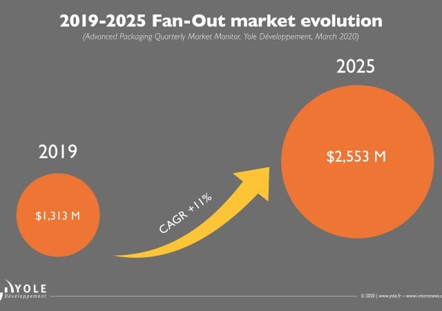
Wafer Level Packaging Reaches New Heights
Fan-out package revenue is expected to surpass $2B by 2025 and fan-in WLCSP revenue to peak to $3B by 2025 as TSMC continues to drive the fan-out market in 5G applications.
Intel Replaces 10+ with Tweaked SuperFin Technology
Intel held their virtual 2020 Architecture Day on August 13th, hosted by Raja Koduri, and the first major topic was Process Innovations, with Ruth Brain as the presenter. Ruth started with a potted history of Intel processing, from the first strained channel at the 90-nm node to the string of 14-nm evolutions.
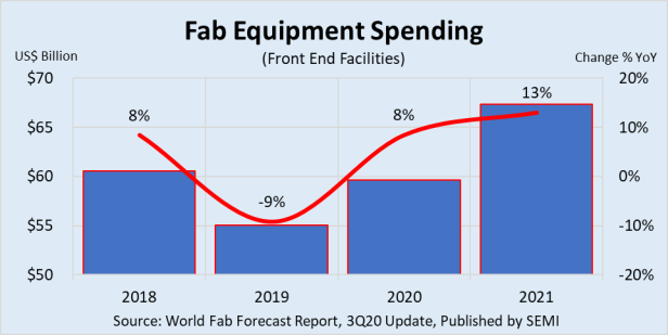
COVID-19 Drives Rise in Global Fab Equipment Spending, SEMI Reports
Soaring pandemic-inspired demand for chips that power everything from communications and IT infrastructures to personal computing, gaming and healthcare electronics will drive an 8% increase in global fab equipment spending in 2020 and a 13% increase in 2021, SEMI announced today in its World Fab Forecast report. Rising demand for semiconductors for datacenter infrastructures and server storage along with the buildup of safety stock as U.S.-China trade tensions intensify are also contributing to this year’s growth.
SUSS MicroTec and DELO Announce Collaboration on Imprint Lithography
SUSS MicroTec and DELO cooperate in the optimization of imprint manufacturing processes for the production of wafer-level optics (WLO). These optics are essential for emerging applications in the automotive and consumer electronics industries, among others.
AKHAN Semiconductor’s Latest US Patent Addresses Diamond Film for Consumer Electronic Displays
AKHAN Semiconductor, a technology company specializing in the fabrication and application of lab-grown, electronic-grade diamonds, announced today that it has been issued a patent by the United States Patent Office (USPTO) generally related to systems and methods for transparent diamond electronics.