The field of photonic integration — the area of photonics in which waveguides and devices are fabricated as an integrated system onto a flat wafer — is relatively young compared to electronics.
Palomar Technologies Moves to New Global Headquarters, Expands Manufacturing Footprint to Meet Growth Goals and Customer Needs
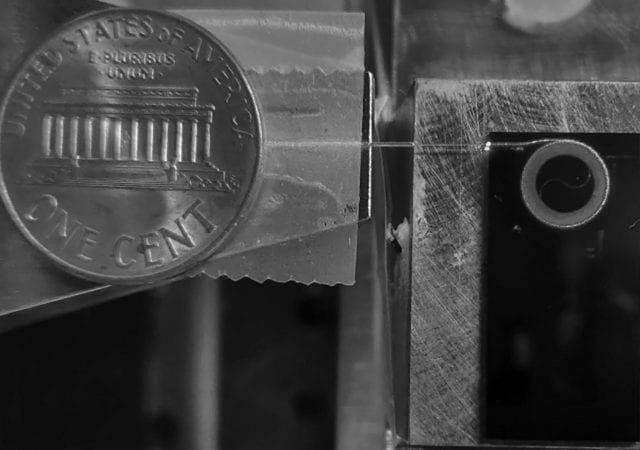
Palomar Technologies, a global leader in total process solutions for advanced photonics and microelectronic device packaging announced that to meet growing customer demand for its solutions around the world, it has moved to a new global headquarters and expanded its facilities to over 110,000 square feet.

Solid State Technology Content Now Available
The content from Solid State Technology is now available through the Semiconductor Digest website.
Eta Compute Announces Production Silicon of the World’s Most Energy-efficient Edge AI Processor
Eta Compute Inc., a company dedicated to delivering machine learning to mobile and edge devices using its revolutionary new platform, announces the first shipment of production silicon for its ECM3532, the world’s first AI multicore processor for embedded sensor applications. This unique multicore device features the company’s patented Continuous Voltage Frequency Scaling (CVFS) and delivers power consumption of microwatts for many sensing applications.
BrainChip Akida Development Environment Now Freely Available to System Developers
BrainChip Holdings Ltd. (ASX: BRN), a leading provider of ultra-low power, high-performance edge AI technology, today announced that access to its Akida™ Development Environment (ADE) no longer requires pre-approval, now allowing designers to freely develop systems for edge and enterprise products on the company’s Akida Neural Processing technology.
Quik-Pak Announces Substrate Development Service
Quik-Pak, a provider of innovative microelectronic packaging and assembly solutions, today announced its substrate design, fabrication and assembly service. Utilizing virtually any substrate type, Quik-Pak can create turnkey solutions for substrate-based assemblies to accommodate customers’ unique packaging requirements, with delivery times at least 50 percent faster than those of competitive services.
Compound Photonics and Plessey Light Up First 0.26 Inch Fully Addressable Integrated microLED Display Module
Compound Photonics US Corporation (CP), a leading provider of compact high-resolution microdisplay solutions for Augmented Reality (AR) and Mixed Reality (MR) applications, and Plessey Semiconductors Ltd. (Plessey), an embedded technologies developer at the forefront of microLED technology for AR and MR display applications, today announced they have produced the first fully addressable microLED display modules resulting from their previously announced strategic partnership to develop and introduce GaN-on-Silicon microLED based microdisplay solutions for AR/MR applications.
‘Atomic Dance’ Reveals New Insights Into Performance of 2D Materials
A team of Northwestern University materials science researchers have developed a new method to view the dynamic motion of atoms in atomically thin 2D materials. The imaging technique, which reveals the underlying cause behind the performance failure of a widely used 2D material, could help researchers develop more stable and reliable materials for future wearables and flexible electronic devices.
Nanowires Made of Tellurium and Nanotubes Hold Promise for Wearable Tech
Wearable tech and electronic cloth may be the way of the future, but to get there the wiring needs to be strong, flexible and efficient. Boron nitride nanotubes (BNNT), studied by physicists at Michigan Technological University, encase tellurium atomic chains like a straw, which could be controllable by light and pressure. In collaboration with researchers from Purdue University, Washington University and University of Texas at Dallas, the team published their findings in Nature Electronics this week.
Emerging Market for Low-Density Panel FO Analyzed
Large area fan-out (FO) remains a hot topic in the industry. There is some confusion over the term “panel” because IC package substrates are processed in panels. The main driver for large area FO panel development is cost reduction because more parts can be processed in a batch. TechSearch International’s latest Advanced Packaging Update report divides the panel market into high-density RDL (≤2μm L/S with multiple RDLs) versus low-density (>5μm L/S with ≤3 RDLs).