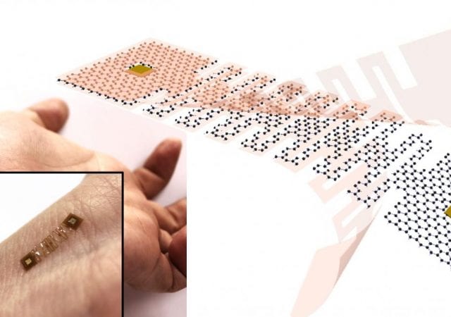
As wearable sensors become more prevalent, the need for a material resistant to damage from the stress and strains of the human body’s natural movement becomes ever more crucial. To that end, researchers at the University of Illinois at Urbana-Champaign have developed a method of adopting kirigami architectures to help materials become more strain tolerant and more adaptable to movement.
Samsung Expands its Commitment to Foundry Customers with the First ‘SAFE Forum 2019’
Samsung Electronics Co., Ltd. today held the first Samsung Advanced Foundry Ecosystem (SAFE™) Forum 2019 in the United States. By sharing the latest technology trends and strengthening cooperation within the foundry ecosystem, Samsung showcased its strong dedication to customers. SAFE Forum is designed to provide an opportunity for SAFE partner companies to directly meet with customers to discuss comprehensive design technology infrastructure, including electronic design automation (EDA), intellectual property (IP), cloud, design service, and packaging, which is critical to efficiently developing and manufacturing semiconductor products.
US Department of Defense to Invest up to $170M in SkyWater’s Domestic Technology Foundry
SkyWater Technology, the innovator’s trusted partner for a competitive edge, announced the US Department of Defense (DOD) is planning to invest up to $170 million for a multi-phase project to enhance microelectronics capabilities for the DoD and the Strategic Radiation Hardened (Rad-Hard) market. SkyWater will be expanding its Trusted Foundry facility to add clean room area and supporting infrastructure to enable this and other complementary technologies. The initial phase is funded at $80 million and SkyWater will leverage this investment to develop a new 90 nm rad-hard electronics production capability to complement its existing 90 nm rad-tolerant offering. In addition, it will fund SkyWater to add copper (Cu) dual-damascene interconnect technology to the facility which marks a significant advancement for the company’s mixed-signal and interposer offerings. Future phases of the effort include options for more advanced microelectronics capabilities.
Big Data Technique Reveals Previously Unknown Capabilities of Common Materials
When scientists and engineers discover new ways to optimize existing materials, it paves the way for innovations that make everything from our phones and computers to our medical equipment smaller, faster, and more efficient. According to research published today by Nature Journal NPG Asia Materials, a group of researchers — led by Edwin Fohtung, an associate professor of materials science and engineering at Rensselaer Polytechnic Institute — have found a new way to optimize nickel by unlocking properties that could enable numerous applications, from biosensors to quantum computing.
Schools of Molecular ‘Fish’ Could Improve Display Screens
Take a dive into what may be the world’s smallest coral reef. Scientists at the University of Colorado Boulder are using a type of material called liquid crystals to create incredibly small, swirling schools of “fish,” according to a study published recently in the journal Nature Communications. The fish in this case aren’t actually aquatic animals. They’re minute disruptions in the orientations of the molecules that make up solutions of liquid crystals, said Hayley Sohn, lead author of the new study.
New Transient-Voltage-Suppression Diodes from STMicroelectronics Deliver Higher Protection in Smaller Packages
In addition to the lower profile, ST’s new 1500W SMB Flat package has transient-power capability equivalent to that of conventional devices in SMC packages, in a footprint more than 50% smaller. The 400W and 600W SMA Flat and SMB Flat devices are fully footprint-compatible with alternatives in conventional SMA and SMB packages. Leakage current is five times lower compared with other TVS diodes on the market, minimizing impact on system operation and power consumption.
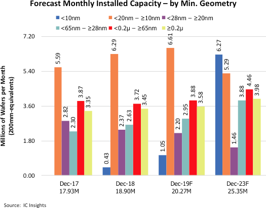
Wafer Capacity by Feature Size Shows Rapid Growth at <10nm
Leading-edge processes (<28nm) took over as the largest portion in terms of monthly installed capacity available in 2015. By the end of 2019, <28nm capacity is forecast to represent about 49% of the IC industry’s total capacity, based on information in IC Insights’ Global Wafer Capacity 2019-2023 report.
Cadence Custom/AMS Flow Certified for Samsung 5LPE Process Technology
Cadence Design Systems, Inc. (NASDAQ: CDNS) today announced that its custom and analog/mixed-signal (AMS) IC design flow has achieved certification for Samsung Foundry’s 5nm Low-Power Early (5LPE) process technology. This certification ensures mutual customers of Cadence and Samsung Foundry have immediate access to a highly automated circuit design, layout, signoff and verification flow needed to design efficiently at 5LPE.
Double Layer of Graphene Helps to Control Spin Currents
Electrons have a negative charge, but they also behave like tiny magnets. This property of electrons, called spin, can be used to transport or store information in electronic circuits. Scientists are looking for ways to create such spin-based electronics, as this is probably more energy efficient than normal electronics. University of Groningen physicist Siddhartha Omar discovered a way to transport spins over long enough distances to make such devices feasible. Furthermore, the material he used enabled him to control these spin currents.
Paving a Way to Achieve Unexplored Semiconductor Nanostructures
Nanowire is a rod-structure with a diameter typically narrower than several hundred nanometers. Due to its size and structure, it exhibits characteristic properties which are not found in larger bulk materials. The study of III-V semiconductor nanowires has attracted much interest in recent decades due to their potential application in nanoscale quantum, photonic, electronic, and energy conversion, and in biological devices, based on their one-dimensional nature and large surface to volume ratio.