The VLSI Symposia are coming up on June 12 – 17, at the Hilton Hawaiian Village in Honolulu, and recently their media associates released the tipsheet describing some of the upcoming papers. The detailed program is available here.
Since the development of mobile phone camera image sensors, they have been a hot topic with continuous evolution to sub-micron pixels, and more recently the move towards self-driving cars (and other ranging needs) is pushing LiDAR systems.
Scanning through the tipsheet, I noticed image sensor papers by Samsung and Sony, and ranging talks from Toshiba and Toppan. In numerical order, starting with Sony:
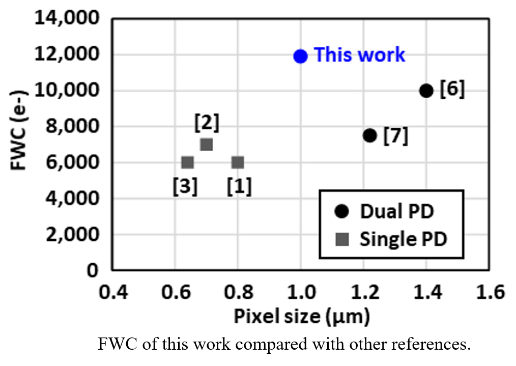
“A 2-Layer Transistor Pixel Stacked CMOS Image Sensor with Oxide-Based Full Trench Isolation for Large Full Well Capacity and High Quantum Efficiency” (Paper T1-3)

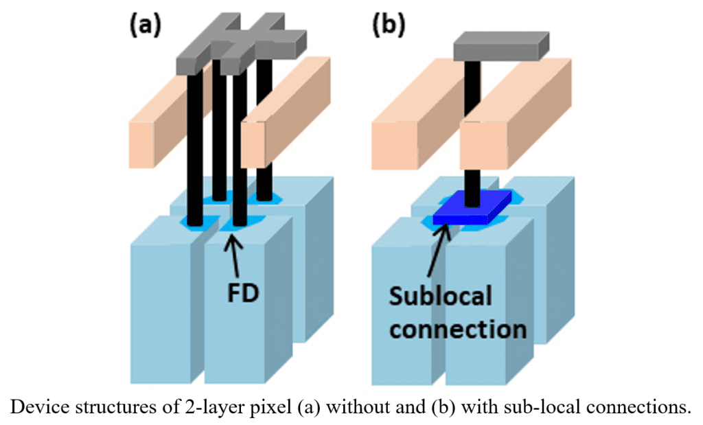
They announce a 1.0-μm dual-photodiode (PD) two-layer transistor pixel stacked CMOS image sensor (CIS) with a high quantum efficiency (QE) and large full well capacity (FWC). The photodiode volumes are increased by using a different silicon layer to the pixel transistors, bonded by a three-dimensional sequential integration process, and multiple floating diffusions are interconnected locally, improving the conversion gain and random noise.
The full-trench isolation uses silicon oxide instead of conventional poly-Si to prevent the isolation absorbing light, increasing the 530-nm QE by 19%. The FWC was measured as 12,000e-, only seen before with larger pixels.

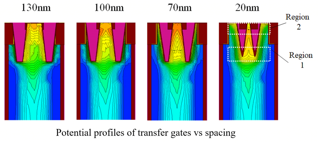
Later in the technology sessions, we have a paper on “A 0.6μm Small Pixel for High Resolution CMOS Image Sensor with Full Well Capacity of 10,000e- by Dual Vertical Transfer Gate Technology” (Paper T8-4).

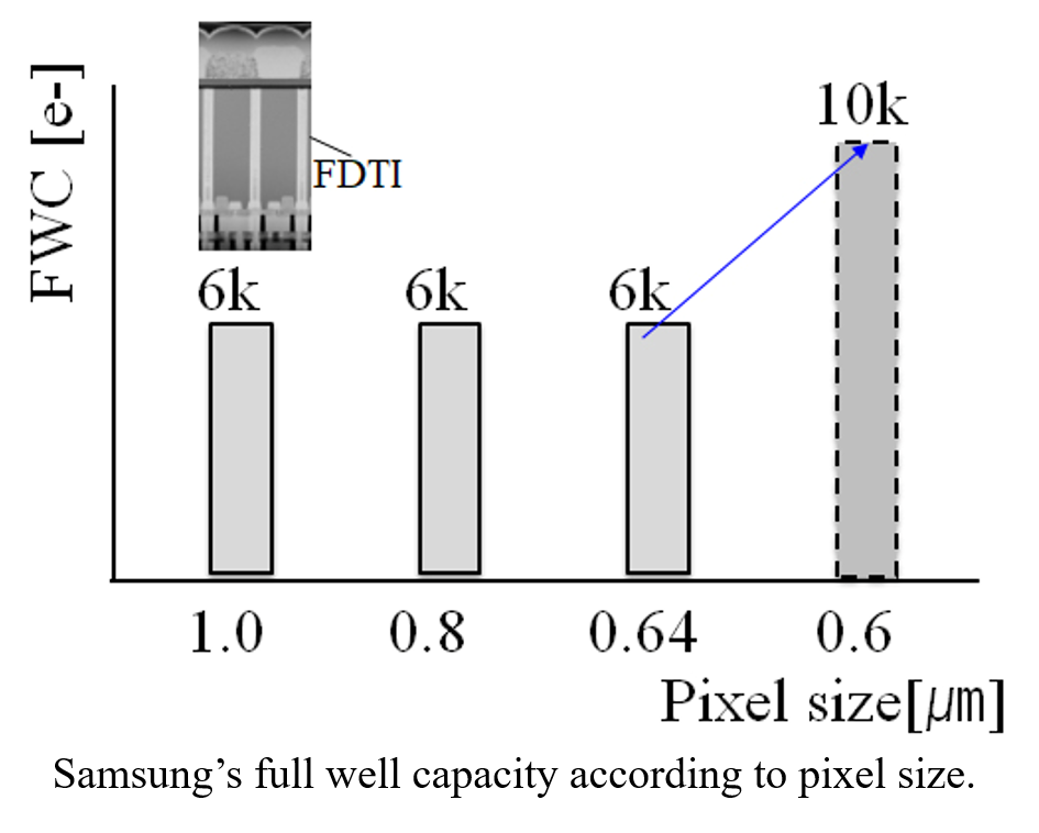
Samsung have developed a prototype 200 Mp image sensor using 0.6μm pixels with a full well capacity (FWC) of 10,000 e- using a dual vertical transfer gate (D-VTG) technology. Compared to single vertical transfer gate, the FWC of the D-VTG increases by 60%, and improves the transfer properties due to the improved controllability of transfer gate voltage.

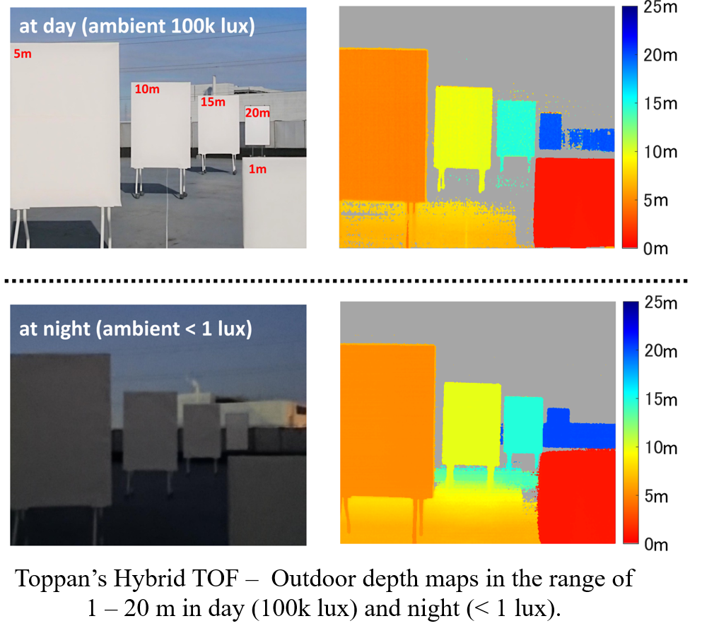
Moving now to the distance ranging papers, Toppan will present “A Hybrid Indirect ToF Image Sensor for Long-Range 3D Depth Measurement Under High Ambient Light Conditions” (Paper C5-2)
It seems that LiDARs and high-resolution indirect time of flight (ToF) image sensors for 3D depth measurement lose precision as distance increases. Toppan, Brookman Technology and Shizuoka University have come up with a new timing scheme for indirect ToF which achieves both long distance and high precision.
The technique uses interference suppression, allowing multiple cameras to work simultaneously in the same field of view, and they apply it in a VGA sensor to achieve a 30 m range with less than 15 cm precision, and up to 100 Lux ambient light. The technology is claimed to be suitable for many uses, including outdoors.

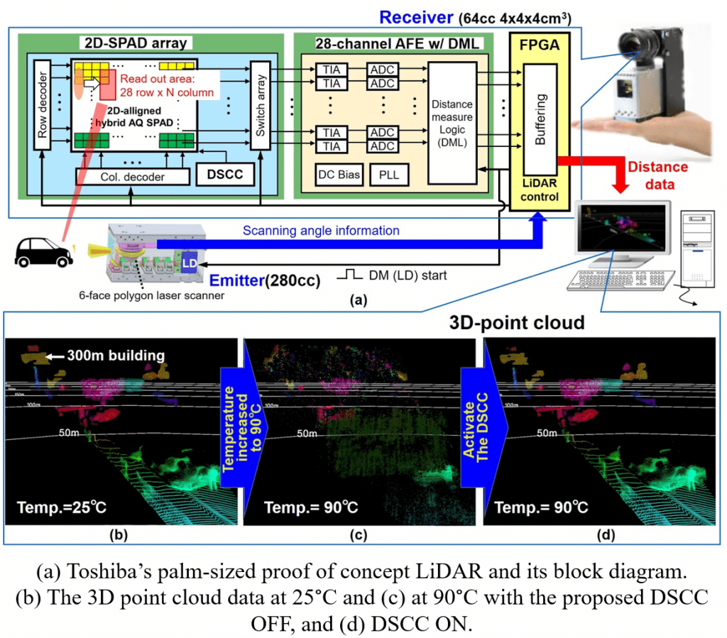
Toshiba’s LiDAR receiver incorporates a 1200 x 84 sensor embedding optimized active-quench CMOS-SPAD pixels within deep trench isolation. Normally the high operating voltage needed for SPADs adds cost with many off-chip components: in this work the system bill of materials is reduced by embedding an on-chip digital background low-voltage control loop (DSCC) which compensates for process and temperature drift of the SPAD array.

There are eleven more image sensor and related papers in the conference:
C05-1 A 640×480 Indirect Time-of-Flight Image Sensor with Tetra Pixel Architecture for Tap Mismatch Calibration and Motion Artifact Suppression (Ulsan NIST, SolidVue)
C05-3 A 4-Tap CMOS Time-of-Flight Image Sensor with In-pixel Analog Memory Array Achieving 10Kfps High-Speed Range Imaging and Depth Precision Enhancement (Tohoku U)
C05-4 Imager with Dynamic LSB Adaptation and Ratiometric Readout for Low-Bit Depth
5-μW Peak Power in Purely-Harvested Systems (National University of Singapore)
C08-4 A 44.3mW 62.4fps Hyperspectral Image Processor for MAV Remote Sensing (National Taiwan University)
C09-1 A 39,000 Subexposures/s CMOS Image Sensor with Dual-tap Coded-exposure Data-memory Pixel for Adaptive Single-shot Computational Imaging (U Toronto)
C09-3 A 100×80 CMOS Flash LiDAR Sensor with 0.0011mm2 In-Pixel Histogramming TDC Based on Analog Counter and Self-Calibrated Single-Slope ADC (Ulsan NIST)
C18-5 Palm-sized LiDAR module with III/V-on-Si optical phased array (Samsung)
T08-1 First Demonstration of High-Sensitivity (NEP<1fW·Hz-1/2) Back-Illuminated Active-Matrix Deep UV Image Sensor by Monolithic Integration of Ga2O3 Photodetectors and Oxide Thin-Film-Transistors (Institute of Microelectronics of Chinese Academy of Sciences, University of Science and Technology of China, Virginia Polytechnic Institute and State University)
T08-2 Low-Noise Multi-Gate Pixel Transistor for Sub-Micron Pixel CMOS Image Sensors (Sony)
T08-3 Wafer Level Pixelation of Colloidal Quantum Dot Image Sensors (imec)
T08-5 Advanced novel optical stack technologies for high SNR in CMOS Image Sensor (Samsung)
In addition, there is a Circuits Short Course on “Fundamentals of Lidar Technology and Latest Developments” by Oichi Kumagai of Sony on the Monday afternoon at 3.30 pm.