DR. PRAVEENA MANIMUNDA, Applications Scientist II, HORIBA Scientific
The semiconductor industry forms the bedrock of modern technology, fueling advancements in computation, communication, and energy efficiency. The continuous drive for smaller, faster, and more energy-efficient devices propels intensive research into novel semiconductor materials beyond conventional silicon. These include two-dimensional materials like graphene and transition metal dichalcogenides (TMDs), quantum dots, nanowires, and advanced alloys. A thorough understanding of the fundamental electronic, vibrational, and optical properties of these materials at the nanoscale is paramount for realizing their full technological potential.
Spectroscopy, the study of the interaction between matter and electromagnetic radiation, offers a powerful and non-destructive means to probe these properties. Leading manufacturers have developed sophisticated spectroscopic instrumentation specifically tailored to address the unique challenges of semiconductor material characterization. This scientific study illuminates the application of key spectroscopic techniques—Raman spectroscopy, photoluminescence (PL) spectroscopy, and spectroscopic ellipsometry—in elucidating the complex characteristics of advanced semiconductor materials.
Methods
This narrative is grounded in established principles of semiconductor physics and materials science, exemplified by the application of advanced spectroscopic instrumentation.
Raman Spectroscopy Raman spectroscopy was utilized to investigate the vibrational modes of various semiconductor materials, employing high-resolution confocal Raman microscopes. Samples, including exfoliated monolayer TMDs (e.g., MoS₂, WS₂), silicon nanowires, and germanium-tin (GeSn) alloys, were excited using lasers of different wavelengths (e.g., 532 nm, 633 nm). The scattered light was analyzed to identify characteristic Raman modes, providing information on:
The frequencies and symmetries of Raman modes serve as unique identifiers for specific materials and their crystalline forms, facilitating material identification and crystal structure analysis. Shifts in Raman peak positions and alterations in intensity reveal the presence of internal strain and the concentration of dopant atoms within the material, offering insights into strain and doping effects. The appearance of specific Raman modes associated with lattice imperfections indicates the presence and type of structural defects, aiding in defect analysis. In nanomaterials such as quantum dots and nanowires, observable changes in phonon frequencies arise due to the spatial confinement of vibrations, demonstrating quantum confinement.
Photoluminescence (PL) Spectroscopy Photoluminescence spectroscopy was employed to study the electronic transitions and band structure of semiconductor materials, utilizing sensitive spectrofluorometers and high-resolution Raman systems equipped with appropriate detectors (e.g., silicon CCD, InGaAs). Samples were excited with lasers of varying energies (e.g., 405 nm, 532 nm), and the emitted light was analyzed as a function of wavelength. PL measurements provided insights into:
The energy of the emitted photons directly corresponds to the energy difference between electronic bands, enabling the precise determination of the material’s bandgap energy. In low-dimensional semiconductors, the strong Coulomb interaction between electrons and holes forms excitons, leading to characteristic emission features, which reveal the exciton binding energy. Emission peaks with energies lower than the bandgap often originate from the recombination of charge carriers at defect sites or impurity levels within the material, indicating defect states and impurities. The wavelength of light emitted by quantum dots and nanowires is strongly dependent on their physical dimensions due to the quantum mechanical confinement of electrons and holes, illustrating quantum confinement effects.
Spectroscopic Ellipsometry Spectroscopic ellipsometry was utilized to determine the optical constants (refractive index, extinction coefficient) and thickness of thin semiconductor films and multilayer structures. This technique measures the change in the polarization state of light upon reflection from the sample surface as a function of incident angle and wavelength. Modeling the acquired ellipsometric data allowed for the extraction of:
The refractive index and extinction coefficient are fundamental parameters that describe how light propagates through and is absorbed by the material, crucial for optoelectronic device design, providing vital optical properties. Precise determination of the thickness of individual layers in thin film devices is essential for controlling their optical and electronic performance, enabling accurate film thickness measurements. Ellipsometry is sensitive to the presence of interfacial layers and surface roughness, offering information about the quality of interfaces in multilayer structures and assessing interface quality. In semiconductor alloys, such as GeSn, ellipsometric data can be used to estimate the relative concentrations of the constituent elements, facilitating compositional analysis.
Data
Illustrative data obtained using advanced spectroscopy on various semiconductor materials is presented below:
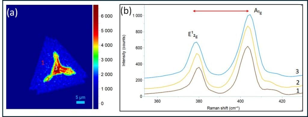
Raman spectroscopy of MoS₂ (FIGURE 1) shows Raman spectra distinguishing between monolayer and bilayer molybdenum disulfide. The characteristic shifts in the in-plane (E¹₂g) and out-of-plane (A₁g) vibrational modes confirm the number of atomic layers and reveal information about the weak van der Waals forces between layers. The absence of significant defect-related peaks indicates a high degree of crystalline perfection.
Spectroscopic Ellipsometry of GeSn Thin Film (FIGURE 2) displays representative ellipsometric parameters (Ψ and Δ) as a function of wavelength, along with the corresponding theoretical fit, for a thin film of germanium-tin alloy grown on a silicon substrate. The extracted spectra of the refractive index (n) and extinction coefficient (k) reveal the material’s optical behavior across the visible and near-infrared spectral regions. The fitted film thickness is a critical parameter for device fabrication. The onset of absorption at lower energies is indicative of the material’s bandgap.
PL Spectroscopy of Silicon Nanowires (FIGURE 3) presents the photoluminescence spectrum of silicon nanowires, showing an emission peak that is shifted to higher energy (shorter wavelength) compared to bulk silicon. This blue-shift is a direct consequence of quantum confinement effects within the one-dimensional nanostructure. The presence of weaker emission bands at lower energies suggests the existence of surface states or defects that can influence the nanowire’s electronic and optical properties.
Click here to read the full article in Semiconductor Digest.