By VAIBHAV TRIVEDI, Senior Technology and Market analyst at Yole Développement (Yole), Phoenix, AZ
Wafer level packaging (WLP) has acquired significant interest and focus in last ten years as the semiconductor industry continues to push for higher performance generation after generation primarily driven by mobile and consumer segment. As Moore’s Law continues to slow down due to increasing difficulty in manufacturing sub 7 nm and below technologies, back-end packaging processes become ever important in addressing the need for low latency, higher bandwidth, and cost-effective semiconductor devices. This article explores current market dynamics in WLCSP, and Fan-out packages, examines supply chain and key players involved in WLCSP and Fan-out markets, and attempts to provide future growth scenarios for wafer level packaging especially on fan-out packages. It also describes drivers for panel-level packaging and current status of panel level manufacturing across key players. This article will also examine novel trends such as chiplets as how IDMs such as Intel and TSMC continue to push new boundaries using fan-out processes as an enabler for heterogeneous solution for years to come.
FO and WLCSP packaging
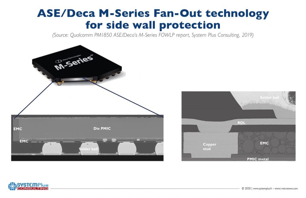
FO (fan-out) packaging began several years ago with limited applications, but it has now found a critical role and rightful place in the high-end packaging sector as a mature, reliable package technology. In fact, TSMC’s InFO form-factors brought FO technology to new heights in 2015/2016 as Apple launched its A10 with InFO-PoP approach. FO packages are primarily used in the mobile and consumer segments, with some proliferation in automotive radar. FO packaging is expected to gain wider adoption as 5G, AI, and autonomous driving take flight in the coming years – and revenue stemming from FO packaging is expected to reach $2.5B by 2025. WLCSP package market also found a new “M-series” product which provides 6 side mold protection with superior board level reliability (BLR) performance. HDFO remains a key growth driver in the FO (Fan out) packaging market.
WLCSP fan-in package market dynamics
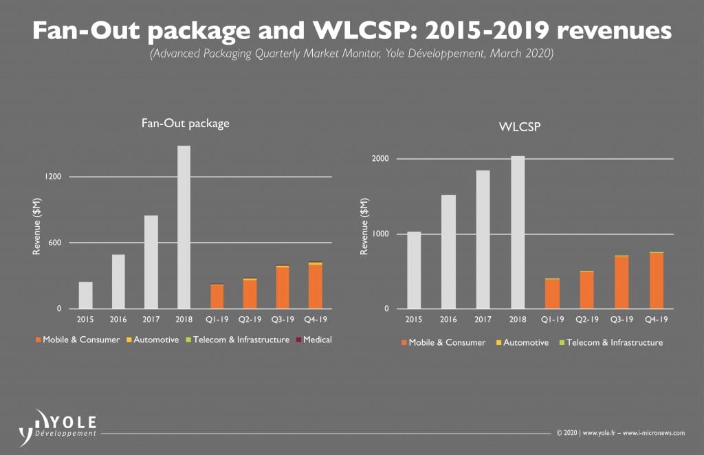
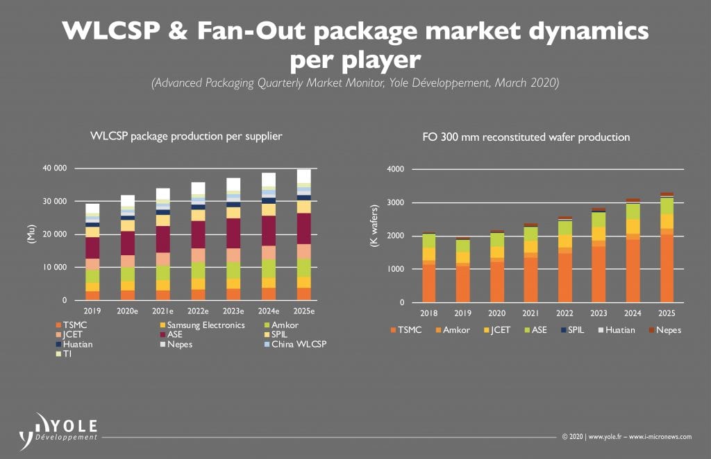
WLCSP package generated record revenue in 2019 at $2B with projected of 5% CAGR over next five years (FIGURE 1). Smartphone OEMs continue to increase WLCSP package usage for many devices such as PMICs, Audio-Codec modules, RF transceivers, NFC controllers, Connectivity modules, and many other applications. WLCSP market is dominated by top OSATs such as ASE, Amkor, JCET, SPIL followed by foundry players such as TSMC, Samsung, Chinese OSATs, and few IDM players. Top OSATs continue to invest in additional WLCSP and bumping infrastructure for 2020 driven by increased IoT demand and adoption of more WLCSP packages in smartphone eco-system.

The outlook for 2020-2025 remains strong and robust as new adoption of WLCSP form factors gains wide adoption in all smartphone/luxury phone form factors. WLCSP market is expected to grow to $3B+ market by 2025. Packaging suppliers continue to enjoy robust 8” and 12” WLCSP demand across various devices. WLCSP has become a mainstream “workhorse” packaging technology for mobile/consumer applications offering lowest cost solution compare to substrate-based packages. In next five years, RF components may also transition to WLCSP type platform compare to wirebond configuration as it provides overall lower module cost as a result of substrate optimization.
Fan-Out package market dynamics
FOWLP package generated $1.3B revenue in 2019 as the semiconductor industry recovered in 2H of 2019 showing very strong OSAT demand (Figure 1). FO (Fan-out) package revenue reduced slightly in 2019 compare to 2018 however, TSMC continues to support Apple application processor with InFO package and InFO-AiP package to arrive in 2H’2020 to support 5G Apple phones.
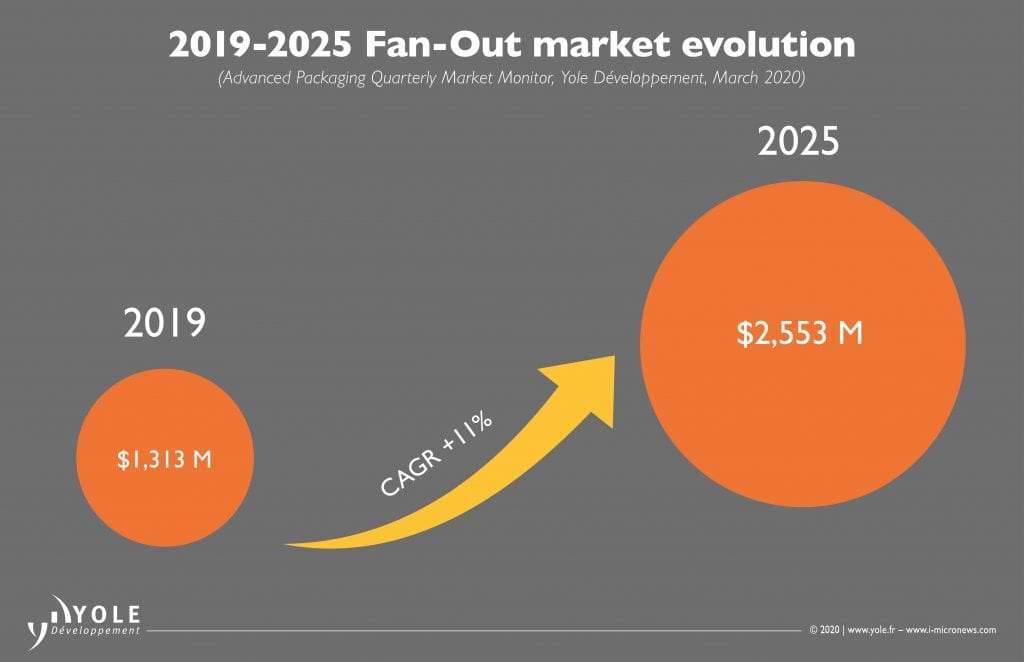
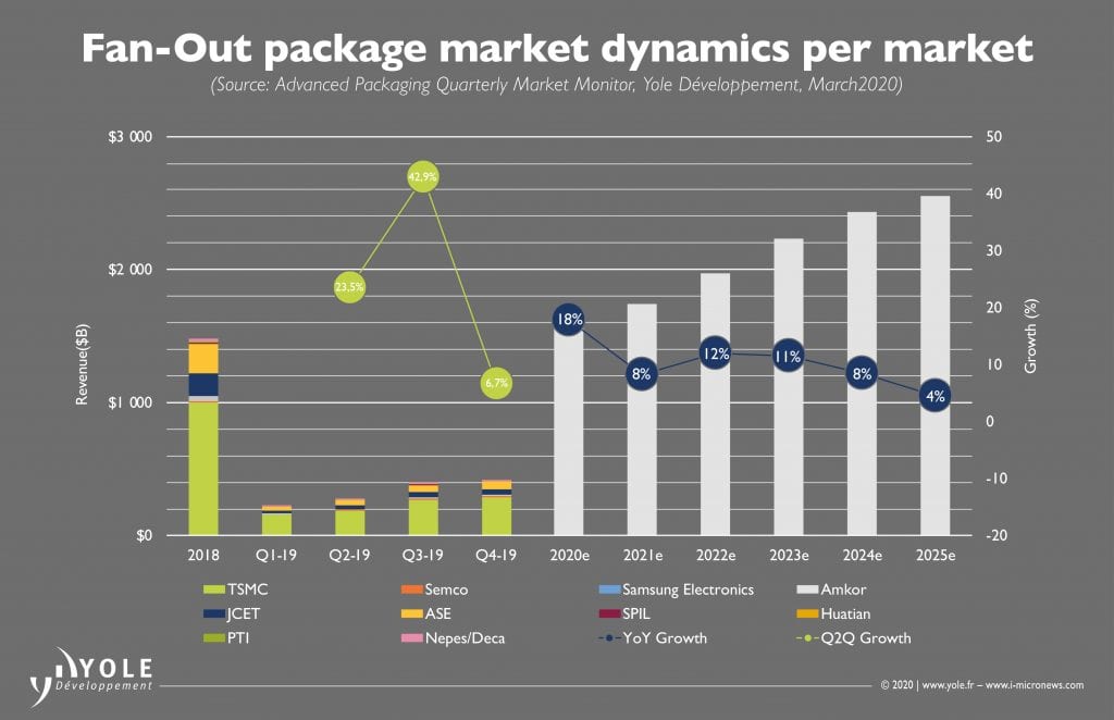
Fan-out package outlook for 2020-2025 remains healthy (Figure 2). Over the next five years, 11% CAGR growth expected for fanout packages mainly driven by TSMC’s InFO offering into iOS eco-system and expected increased adoption of HDFO (High-Density Fan Out) designs by other top phone OEMs besides Apple in coming years. Fanout package market is expected to grow to $2.5B+ by 2025. Fan-out package configurations continue to compete with more traditional fcCSP based designs as the latter offers more reliable and lower cost solution. Fan out remains a niche technology with few key players such as TSMC, Samsung, ASE, JCET, and PTI (Figure 3). 5G mmWave adoption could contribute to increased number of fan-out packages especially for the OSAT segment (RF segment). Core FO to see slow growth and expect to remain flat as many device requirements can be fulfilled by fan-in WLCSP and more reliable fcCSP configurations. Fan-out CapEx expected to grow as more phone OEM players expect to adopt HDFO platform for application processors with surge in TSMC CapEx expected in addition to
Panel level market dynamics
FO-PLP technology driven mainly by Semco, Samsung Electronics, PTI, and ASE/Deca Technologies with ~3% of packages being manufactured on panel line in 2019 with projected increase to 7.5% by 2025. Semco sold its FO PLP line to Samsung Electronics in mid 2019.
Samsung to optimized recently purchased Semco line to additional package line up on fan-out configurations with possible inflection point in 2020. OSAT industry is in process of narrowing on panel size as 600×600 is being adopted by ASE as they start qualifying panel line production. Samsung Electronics supporting its Galaxy watch with PLP platform and possibility to expand this to Mobile platform devices as well as it competes with TSMC to provide back-end solutions. Samsung continue to fully utilize the panel line bought from Semco and plan for future fan-out devices for 2021 and beyond using the Semco panel line with focus on mid end smartphone APUs. PTI has committed to significant Cap Ex in 2020 to expand its panel manufacturing for Fan-out based packages with more heterogeneous multi-die integration focus.
TSMC goes “all-in”
TSMC announced unprecedented $1.5B CapEx investment in 2020 for advanced packaging business specifically geared towards SoIC, InFO variants, and CoWoS product line with estimated ~$300M for InFO (PoP/AiP/OS/MS) product line. TSMC started manufacturing Apple APU on InFO platform in 2016 disrupting the supply chain as substrate suppliers and OSAT lost this Apple APU business to TSMC. TSMC continues to “bite” into traditional OSAT business for Apple APU PoP assembly and Antenna in Package module for 5G Apple phones with its InFO product line. Intel recently unveiled its Co-EMIB architecture using “chiplet” type face to face interconnect scheme to be used in mobile and high performance applications.
Supply chain for Wafer Level Packaging
WLCSP package market is dominated by top OSATs such as ASE, Amkor, JCET, and SPIL (Figure 4). 8” WLCSP continue to remain in high volume production as many devices do not require highly advanced Si node. WLCSP services consist of bumping and die processing services and can include test as a turn-key business. Majority of WLCSP packages use 1L RDL structure while few use 2L RDL configurations. In next five years, top OSATs will enjoy higher demand for WLCSP packages as more functional devices are converted to WLCSP platform in smartphone eco-system and fast growth of IoT infrastructure.
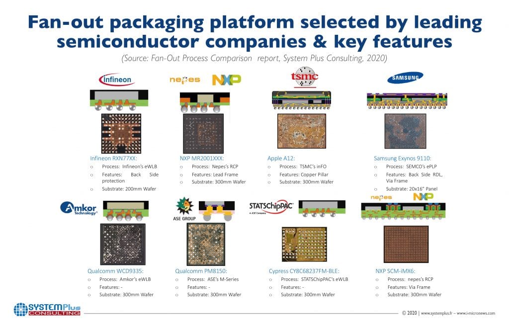
On the contrary, supply chain for fan-out level packaging remain complex (Fig. 4). TSMC continues to enjoy its superior position in offering high density solutions such as InFO-PoP for Apple AP solutions and continues to refine its processes and package offering generation after generation. In this regard, TSMC is taking OSAT and substrate supplier market share for Apple AP devices and also Antenna-In-Package (AiP) devices slated to be used in Apple 5G phones later this year. This lines between a foundry and an OSAT continue to get blurry as shown by TSMC’s advancement in providing “one stop” services impacting business for substrate and OSAT players. Samsung remains another high density fan-out player which recently acquired Semco’s PLP line and there remains high probability that it will be used to produce more fan-out highly integrated packages for its smartphone segment as well. ASE and JCET remain strong OSAT players for fan-out packaging solutions offering multi-die SiP type packages and ASE’s FoCoS product line-up targeted for high end applications. PTI continues to invest in its PLP line expecting to get into high density applications as more phone OEMs plan to adopt this platform in coming years. Figure 5 shows the fan-out packaging platform selected by leading semiconductor companies and key features.
Novel Fan-out packaging form factors
In last few years and in coming years, we expect novel fan-out package form factors such as Deca M-Series (Figure 6) with 6S (6 sides) protection design to gain popularity due to superior BLR (board level reliability). TSMC’s InFO product line up also will include InFO-AiP packages in addition to InFO-PoP, InFO-MS, and InFO-OS. TSMC advanced packaging roadmap provides a glimpse of future as it plans to use SoIC (System on Integrated Chips) as its next integrated solution offering for mobile and high end applications.
TSMC has successfully manufactured APU from 2016 to 2019 on InFO-PoP platform. As chiplet design approach and heterogeneous integration trend continues for next several years, TSMC plans to implement SoIC (System on Integrated Chips) on various mobile and high end applications to be able performance required for 5G computing and new applications of HPC. TSMC SoIC design has potential to cannibalize additional business away from OSATs for FO-SiP applications. In addition to increasing iOS ecosystem content with InFO packages, TSMC may get additional phone OEM customers with fan-out platforms to be adopted for APU modules as race for miniaturization and higher bandwidth continues. In summary, with its mature InFO product line-up, and increased investment in SoIC package infrastructure with chiplet paradigm shift over next 3-5 years, TSMC is in robust position to take advantage of the heterogeneous integration revolution
Fan-out packaging as an enabler for chiplets and heterogeneous integration
As we look at the next five years, heterogeneous integration trend will intensify to support 5G, AI, and IoT megatrends. Fan-out processes and technology serve as a foundation for advanced back-end integration and will be an enabler for chiplets type heterogeneous integration of the future. Intel, TSMC, and Samsung will continue to push the technology envelope to enable various 3D IC heterogeneous integrated package designs of the future. In this race to achieve high density heterogeneous integration, OSATs will also up-level their capability to compete in this lucrative market of high end advanced packaging for coming years.
Yole Development advanced packaging monitor offering
Yole Development has begun publishing, in quarterly instalments, a monitor containing world-class research, data, and insights pertaining to FO and WLCSP packaging markets. This monitor will analyse the WLP package market’s evolution in terms of revenue, shipments, capex, market pricing, capacity, application & process technology mix, and supplier market share. In the future, Yole Development will extend its coverage to 2.5/3D packaging, and FC packaging.
About the author


Vaibhav Trivedi is a Senior Technology & Market analyst at Yole Développement (Yole) working with the Semiconductor & Software division. Based in the US, he is a member of Yole’s advanced packaging team and contributes to analysis of ever-changing advanced packaging technologies. Vaibhav has 17+ years of field experience in semiconductor processing and semiconductor supply chain, specifically on memory and thermal component sourcing and advanced packaging such as SiP and WLP. Vaibhav has held multiple technical and commercial lead roles at various semiconductor corporations prior to joining Yole.