Largest Series A funding for photonic computing in Europe will accelerate commercial rollout of light-based processors to address AI’s escalating energy and scalability crisis.
Packaging
SEMI Southeast Asia Appoints Dato’ Bock KL, Sandisk, as New Regional Advisory Board Chairman
SEMI Southeast Asia announced the appointment of Dato’ Bock KL, Senior Vice President, Global Flash Backend Operations, Sandisk, as the new Chairman of the SEMI Southeast Asia Regional Advisory Board, succeeding KC Ang.
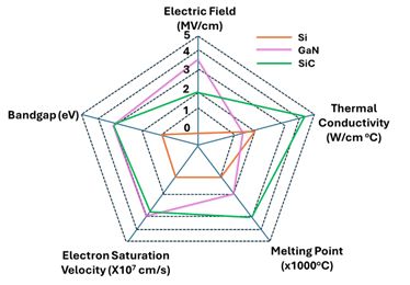
SiC and GaN: The Superior Alternatives Powering Our Energy-Efficient Future
SiC and GaN deliver exceptional performance in demanding applications such as inverters, battery charging systems, and DC-DC converters, offering minimal energy loss and enhanced heat dissipation.
Accelerate Failure Analysis of Heterogeneously Integrated Packages with AI-Powered Correlative Microscopy
A three-step physical failure analysis process dedicated to analyzing fine structures and defects in hybrid bonding and FOWLP packages demonstrates high accuracy and precision, while AI-powered reconstruction accelerates the speed of 3D X-ray scans.
Smartkem Announces Preliminary Joint Development Agreement with Manz Asia
Smartkem today announced that it has entered into a preliminary Joint Development Agreement (JDA) with Manz Asia, a pioneer in advanced packaging equipment for the semiconductor industry.
Nordson Test & Inspection Expands Partnership with Distributor smartTec Nordic A/S
Nordson Test & Inspection today announced that smartTec will expand distribution of X-Ray and Test Solutions to include Denmark, Norway, Finland, Sweden, Latvia, Lithuania and Estonia.
Microchip Partners with Nippon Chemi-Con and NetVision
An automotive industry transition is underway to replace proprietary camera connectivity with solutions based on the open and interoperable Automotive Serdes Alliance Motion Link (ASA-ML) standard driven by over 150 member companies worldwide.
Onto Innovation Announces Agreement to Acquire Semilab International’s Materials Analysis Business
Acquisition adds unique materials characterization technology for advanced nodes, advanced packaging and compound semiconductor applications.
3IT Purchases ClassOne Technology Solstice LT Advanced Plating System for Advanced Packaging R&D
First Canadian customer installs ClassOne system at 3IT research center, enabling access to Solstice’s copper and indium plating capabilities by academic and industrial partners.
3D Printing Breakthrough Paves Way for Next-Gen Medical Devices and Stretchable Electronics
Researchers at The University of Texas at Austin have developed a fast, precise new 3D printing method that seamlessly merges soft and hard properties into a single object using different colors of light.