Pete Singer, Editor-in-Chief
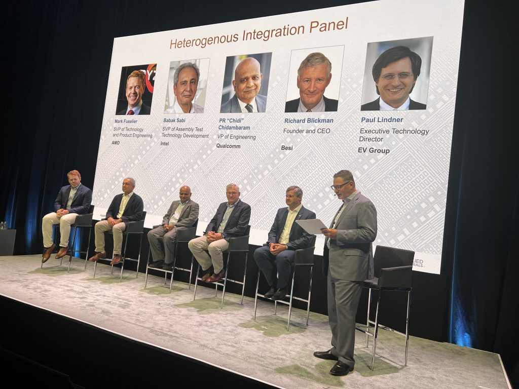
At SEMICON West last week, Applied Materials hosted a panel of experts that focused on emerging trends in heterogeneous design and integration using advanced packaging technology. The panel featured senior technology leaders from AMD, Intel and Qualcomm as well as leading hybrid bonding solution providers Besi and EV Group. The panelists explained why and how heterogeneous integration will drive improvements in semiconductor and system performance, power efficiency, form factor and time-to-market. The panel was moderation by Vincent DiCaprio, Vice President, Business and Corporate Development Heterogeneous Integration and ICAPS, Semiconductor Products Group, Applied Materials. The panelists were:
- Mark Fuselier, SVP of Technology and Product Engineering, AMD
- Babak Sabi, SVP of Assembly Test Technology Development, Intel
- PR “Chidi” Chidambaram, VP of Engineering, Qualcomm
- Richard Blickman, Founder and CEO, Besi
- Paul Lindner, Executive Technology Director, EV Group
The following is an excerpted and edited report of that discussion.

DiCaprio: Let’s start with Mark. Beginning with the early adoption of heterogeneous design and integration with chiplet-based products going back to 2017 with the Zen2 EPYC server processor called Naples, can you talk about why AMD has embraced this approach and what role it has played in enabling the roadmap?
Fuselier: It started out as looking at cost and how we could save by really disaggregating the SoC into pieces and then bringing it back together in a package. And that was really Zen in the data center as you mentioned. Then as we started to get familiar with chiplets, we realized there’s much more opportunity there. The second generation for us is really bringing memory much closer to logic. That was first done with HBM in the graphic space, but then more recently as we introduced with 3D hybrid bond, bringing SRAM much closer to the CPU and through 3D stacking. The third generation that we see is even more exciting and that’s where we can enable true heterogeneous integration, really optimizing our chiplets for either CPU or GPU compute, bringing memory on board as well. It really becomes an architect’s dream of being able to optimize for each workload in the compute space.
DiCaprio: Qualcomm is one of the biggest consumers of both wafer fab and packaging service driven primarily by high performance mobile chip sets. Mark described how AMD is leveraging heterogeneous integration for client and data center. Chidi, can you talk about how this approach is being adopted in the mobile space?
Chidambaram: I’ve been at Qualcomm for 15 years and every year we’ve released a cell phone. Cell phones, as you know are super high volume products that are very competitive at a consumer level in terms of cost and yield.
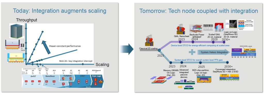
For us to continue to have a phone every 15 years for the next 15 years, we need innovation beyond Moore’s Law. On the graph (Figure 1 left) on the X-axis, I’m showing scaling as one of the components and you can see the dots are getting sparser, right? Five years ago, I knew that gate- all-around would be the technology of 2022, but five years from now I’m not sure what we are going to do.
This uncertainty is going to lead to sparseness in the nodes in the future. We need to go to the vertical axis where I see integration and the throughput being a key vector as opposed to scaling. As we move from scaling to throughput, we are walking in the two-dimensional space between the horizontal to the vertical. That’s really where I think innovation has to happen for us to continue to deliver the user experience that people have to come to expect from us.
The other chart (Figure 1 right) shows how we can get this integrated. We are thinking a lot about it. We don’t have a product yet because it doesn’t meet our cost requirements. Hopefully this event will help get the cost to the point where we’re going to see cell phones doing this in the near future.

DiCaprio: Intel is in a unique position with a business model that’s passed chip design, internal manufacturing, and a growing external foundry business. Babak, if you look at the approach from the manufacturing perspective, can you talk about some of the key technologies that are needed to continue progress in heterogeneous integration?
Sabi: We want to bring everything together at the absolute lowest latency and the highest bandwidth. For those of you who are engineers, this is an interconnect problem. So packaging is all about interconnects and you can think about interconnects as you stack chips on top of each other, which you would like to use hybrid bonding. This is what I call the vertical interconnection.
Then you want to connect the chips together, that’s the lateral interconnect, and you want to make that as dense as possible. In order to be able to do that, you are going to need some new innovation beyond what we have in wafer level assembly. In the AI world, we’re talking about huge complexes.
This is where I think that the glass subset is going to be become extremely important, allowing us to put these huge complexes together and you can completely eliminate the interposer and just go directly from your chips and connect them together. I know we all love copper, but eventually copper is going run out of gas for high speed communication. And we’re going to have to move into what I call optical area.
This is coming. By the end of this decade, we’re going to start seeing optical and we are going to see it in many different formats. Looking into future, what you’re going to see is that you are going to replace your electrical mesh with an optical mesh where you do die-to-die communications using optics. That’s going to bring a huge performance and power reduction in the future.
DiCaprio: Hybrid bonding is clearly a critical capability to enable the next generation of innovation in HI. Richard, while we have seen hybrid bonding rolled out in a few applications, many in the industry are wondering when will it be adopted on a larger scale? Can you talk about your view and the adoption curve and which application will be driving this?
Blickman: The issue is, of course, ever smaller design geometry. Placement accuracy is becoming ever more critical. Even more critical is the handshake between assembly, interconnect and the front end. So that step, we’re in very early stages in bringing the design of the end interconnect on chip level and how to connect that either chip-on-wafer or chip-on-chip. You see in this graph (Figure 2) some cases we have projected for the coming years, the adoption rate of hybrid bonding.

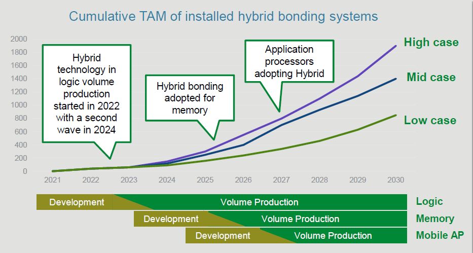
We are in a very early stage of that adoption, but it works. In the last two years, we’ve demonstrated that there are designs which are in high volume markets today. But as with all these technologies simply compare when flip chip came to mainstream, and that was about 23 years ago. It took many years before that really took a major part of that market.
And simply ever smaller design geometries challenge the existing technologies. We know one thing with hybrid bonding, it’s a wonderful process. It’s much easier than doing that with a reflow process at the same time. That bodes very well for hybrid bonding. On the other hand, it has to be more accurate. Particles are one of the biggest enemies. So how to design equipment at the same time in ever smaller geometries.
And then the next step easily said, let’s put them all together in a chiplet architecture. Simply imagine how you place all these different dies in the accuracies required, which is now in the nanometer space. We are very proud that we can deliver machines for production with 200 nanometer accuracy, glass in glass, even below that, we’ve shipped the first system with 100 nanometers.
There are many new challenges which simply have an impact on how this will find its way into the mainstream. But as you’ve heard, the advantages are so numerous that it’s not a question if it will happen, but it’s more a question of timing.
DiCaprio: We’ve seen wafer to wafer hybrid bonding used in CMOS image sensors for several years, and it also appears to be gaining momentum in 3D NAND. Paul, can you give us some insights into the applications and markets that are driving the adoption of wafer to wafer bonding?
Lindner: At EVG, we really view wafer bonding as a scaling booster, as a possibility to transfer active layers from one wafer to another to gain access to the backside of wafers. We were part of the adoption of wafer bonding from the backend to the front end in any device.. even with SOI wafers, which are bonded wafers. The cleanliness challenge and other challenges have been mastered on the wafer level bonding space. The image sensor was the first device adopting the fusion bond initially for the so-called backside illuminated image sensor, which essentially gives access to the backside of the photo diodes so they’re not obstructed by the wiring and gives a greater sensitivity of the sensor.
Later on, the hybrid bond was adopted to integrate memory or logic. Going forward, we also see in the market 3D NAND flash adopting wafer bonding, the hybrid bonding process particularly. We expect if die size is small, if the dies are similar and redundancy can be designed into the dies, that wafer bonding can be adopted for more memory applications going forward.