Contributed by Dick James, Fellow Emeritus, TechInsights
The VLSI Symposia were held on June 12 – 17, at the Hilton Hawaiian Village in Honolulu, and the first paper in the Technology Symposium was from Intel, “Intel 4 CMOS Technology Featuring Advanced FinFET Transistors Optimized for High Density and High-Performance Computing” [1].
Intel held a briefing before the conference, which the technology press took advantage of with posts by Anandtech, Semiwiki, WikiChip Fuse, and Real World Technologies that I know of, so the overall topic has been well covered.
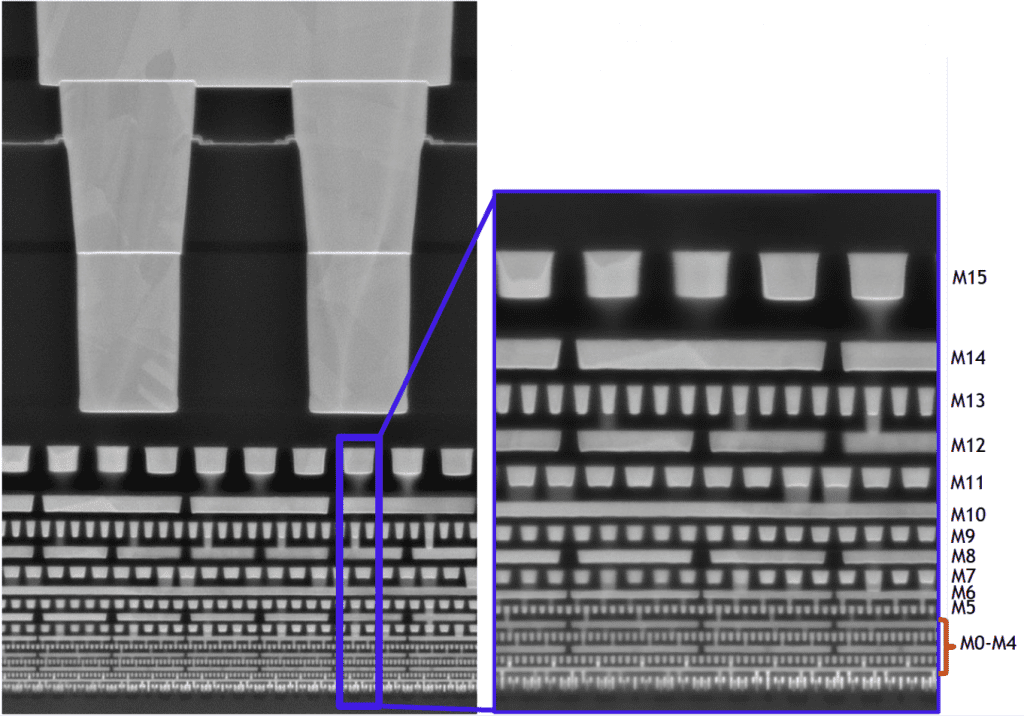
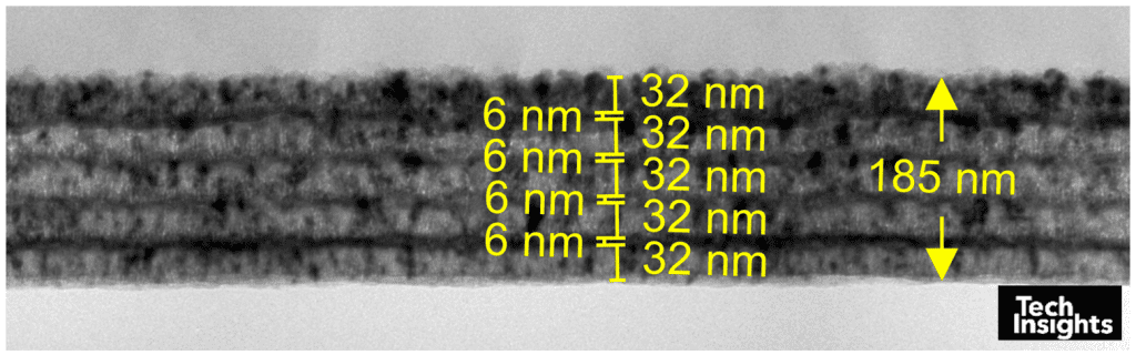
Consequently, rather than repeat the details already well reported, I thought I would focus on the interconnect, which has been relatively lightly reviewed. Below is a TEM image of the stack.

To quote the paper, “The interconnect stack is optimized for RC and via resistance without compromising EM”. Design rules have been modified to match M0 pitch with the fin pitch, and M1/M3 with the contacted gate pitch, and M2/M4 (also parallel with the fins) are at a simple 1.5 multiple of the fin pitch.

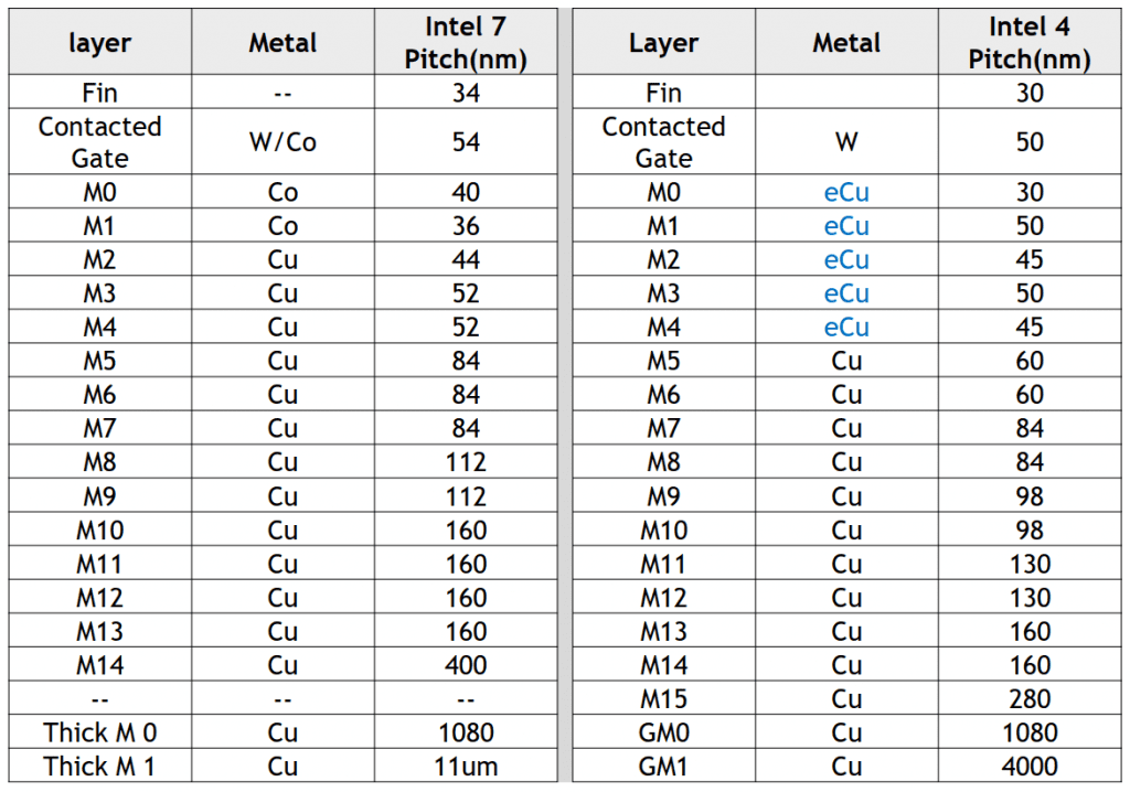
Self-aligned quad-patterning (SAQP) is used to pattern M0, and the other dense metal layers are relaxed enough (at this scale, a relative term) to be dual-patterned, but “EUV (is) used extensively across multiple layers”. If EUV is not actually used for line definition, then it’s likely used for the cut masks – our analyses show that three cut masks were used for the fins and four for M0 in the Intel 10SF and 7, so good opportunities for replacement by EUV. Add in contacts and vias, and we can see clear benefits from EUV.
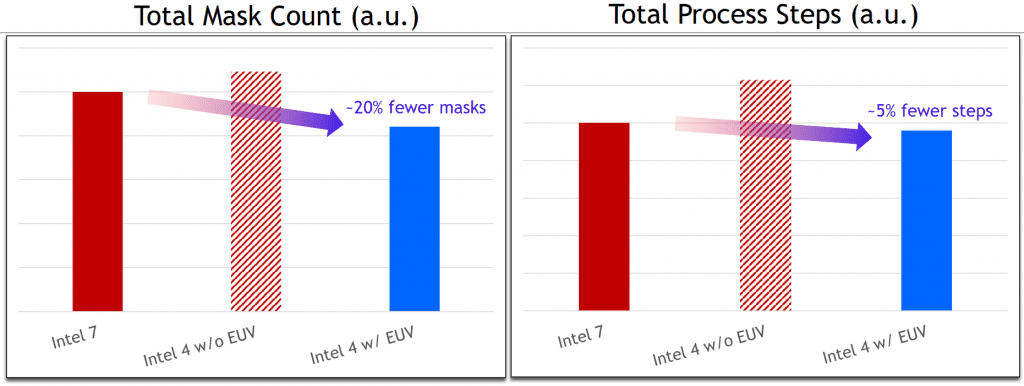
We are given no specific details of EUV use, but Intel claims a 20% reduction in mask count, and 5% in process steps:

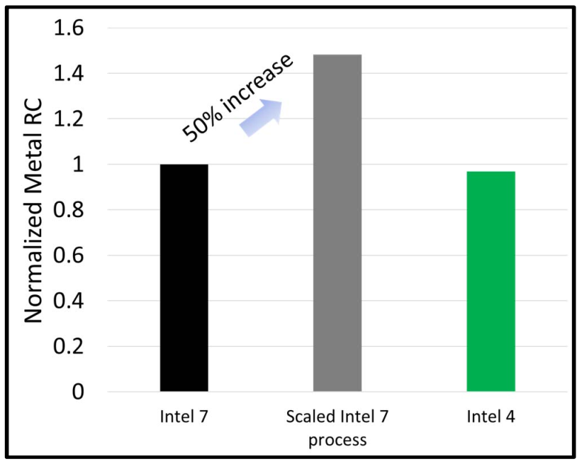
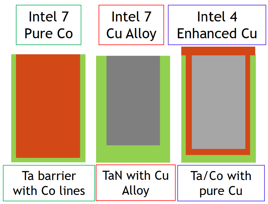
We can see from the design rule table above that M0 – M4 now uses eCu (enhanced copper), and M0/M1 no longer use cobalt. This enables the metal RCs to stay similar to the Intel 7 node despite the dimensional changes.

At 10-nm, Intel claimed that the use of cobalt for contacts reduced contact line resistance by 60%, and using it for M0/M1 reduced via resistance by 2x, and improved electromigration (EM) 5 – 10x.
While those are obvious advantages, clearly cobalt has not proved to be a long-term solution, as we now have eCu, which is Intel-speak for reflow-copper lines with a tantalum barrier, and cobalt liner and cap.

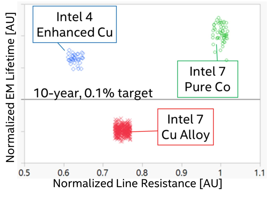
As shown in Fig. 3, eCu has better RC properties, and it also has EM characteristics almost as good as cobalt:

We know that copper with a Co liner and cap has been around for a number of years, so it is not a new technology. Reliability papers have demonstrated the benefits of cobalt liners and cap [2][3], and Applied Materials launched their Endura Volta system for this technology in 2014 [4]. At their press conference at Semicon West that year, they said that there were 90 systems in the field, so we expected to see the technique soon after that.
When we looked at the Apple A9 the following year, in TSMC’s 16FF process, the M1 – M3 layers had Co liners and caps:

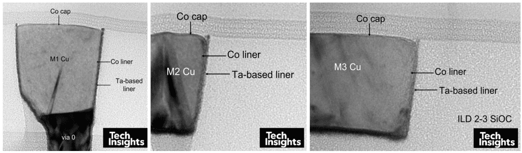
And in fact, it has been used in the minimum pitch metals every generation since then, including the N5:

Intel may have their own tweaks for their eCu process, but in essence it looks as though they had a bit of a misstep using cobalt metallisation in their 10-nm processes. There is still a place for cobalt, though, both TSMC and Samsung have cobalt contacts in their 7- and 5-nm products.
Reportedly Intel 4 has reverted to single-damascene tungsten contacts; the paper states “Enhanced metallization techniques, and barrier/liner scaling enables single damascene patterning in the VCX-M0 layers and allows process simplicity, better reliability, and yield.”
In the next figure we have reversed Fig. 1 to be a bright-field image and zoomed in on M0 – M4 and the transistors:

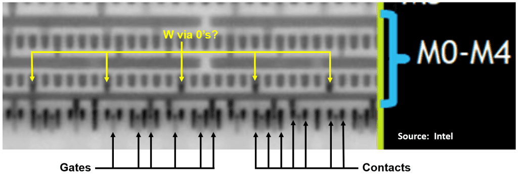
We can see the typical dark image density given by tungsten in the contacts, but I am intrigued by the dark shading in the via 0’s connecting to M1 – it almost looks as though they could be tungsten too. In which case, we have single damascene used for contacts, M0, via 0, and M1.
With respect to the layout, design rules have been changed to a stricter gridded architecture which places line ends and vias on a grid. In the 7-nm process minimum spacing was defined for vias and line ends, but not line end position, creating variable and hard-to-monitor overlaps with adjacent metal layers, and the consequent unpredictable capacitive coupling.

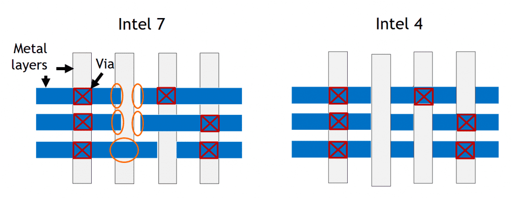
These new rules are claimed to reduce pattern variability and optimize the design flow for the auto-place and route, increasing yield.
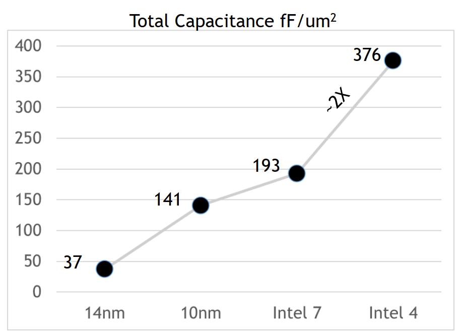
Intel has also updated their metal-insulator-metal capacitor (MIM cap) layer, almost doubling the areal capacitance from Intel 7:

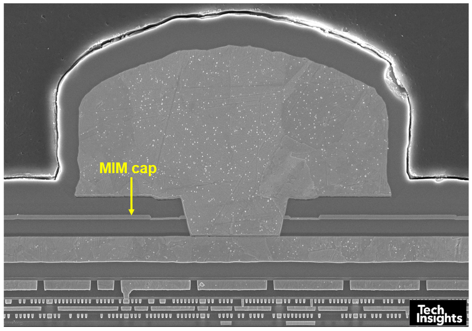
In the Alder Lake (Intel 7), the MIM cap sits almost at the top of the metal stack, under the top redistribution layer.

The MIM-cap layer itself is a five-layer stack of titanium nitride plates sandwiching four dielectric layers, one HfAlO and three HfZrO:

To almost double the capacitance, that implies more plates (and presumably a thicker capacitor), or thinning the dielectric, possibly increasing the dielectric constant, or a combination of the three. Historically, Intel has added a plate layer every generation.

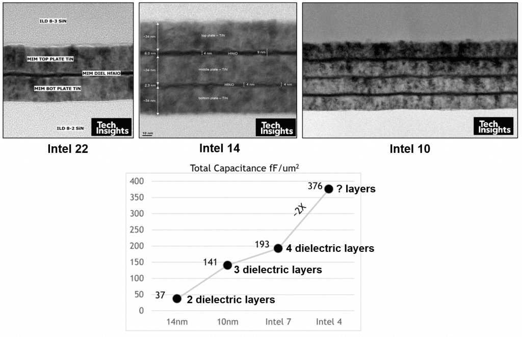
Looking at the graph above, the number of layers obviously has an effect, but there is more going on than just layer count. It seems unlikely that Intel 4 will have eight dielectric layers/nine plates, but we will have to see.
However, if we go back to the 2020 Architecture Day, when the SuperMIM capacitor was launched, Ruth Brain said “The final innovation is new super-MIM (metal-insulator-metal) capacitor. When compared to the industry standard, it delivers a 5x increase in capacitance in the same footprint, driving a voltage reduction that translates to dramatically improved product
performance. … This innovation is enabled by a new class of high-k dielectric materials stacked in ultra-thin layers, just several Ångstroms thick, to form a repeating super-lattice structure.”

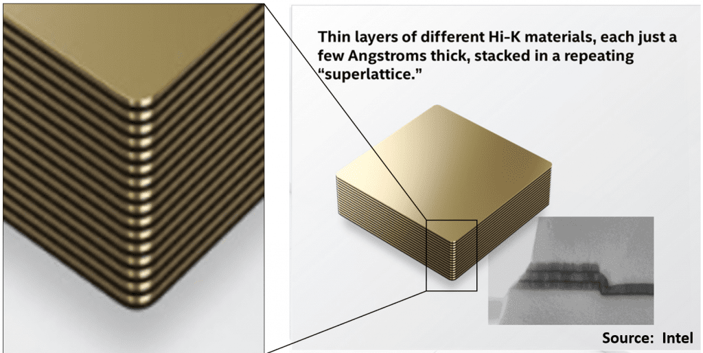
It’s clear that the Intel 7 MIM cap does not have ultra-thin layers just several Ångstroms thick, so maybe we will see SuperMIM in the Intel 4. The first product is their Meteor Lake processor, so we look forward to that!
References
1. B. Sell et al., “Intel 4 CMOS Technology Featuring Advanced FinFET Transistors Optimized for High Density and High-Performance Computing”, VLSI 2022, pp. 282 – 283
2. H.K. Jung et al., “Formation of Highly Reliable Cu/Low-k Interconnects by Using CVD Co Barrier in Dual Damascene Structures”, IRPS 2011, pp. 307 – 311
3. A.H. Simon et al., “Electromigration Comparison of Selective CVD Cobalt Capping with PVD Ta(N) and CVD Cobalt Liners on 22nm-Groundrule Dual-Damascene Cu Interconnects”, IRPS 2013, pp. 3F.4.1 – 3F.4.5
4. K. Shah et al., “CVD Co-Based Metallization for <22nm Cu Interconnects”, Applied Materials Nanochip Tech Journal, Vol. 12, Issue 2, 2014