Semiconductor equipment manufacturer ClassOne Technology announced the sale of its Solstice electroplating system to Yee Wei Co., Ltd , a semiconductor manufacturing foundry based in Taiwan. The Solstice will be installed in Yee Wei’s manufacturing facility in Toufen City, Taiwan. The Solstice family of wet-processing tools includes the 8-chamber Solstice S8, the 4-chamber Solstice S4 and the 2-chamber Solstice LT. The Solstice platform was specifically designed for ≤200mm wafers, which are used in compound semiconductor, emerging technologies, and numerous other fabs worldwide.
Researchers Repurpose Failed Cancer Drug Into Printable Semiconductor
Many potential pharmaceuticals end up failing during clinical trials, but thanks to new research from the University of Illinois, biological molecules once considered for cancer treatment are now being repurposed as organic semiconductors for use in chemical sensors and transistors. Organic semiconductors are responsible for things like flexible electronics and transparent solar cells, but researchers are working to expand their use in biomedicine and devices that require interaction between electrically active molecules and biological molecules.
New Lattice CrossLinkPlus FPGAs Accelerate and Enhance Video Bridging for MIPI-based Embedded Vision Systems
Lattice Semiconductor (NASDAQ: LSCC), the low power programmable leader, today introduced the CrossLinkPlus™ FPGA family for MIPI D-PHY based embedded vision systems. CrossLinkPlus devices are innovative, low power FPGAs featuring integrated flash memory, a hardened MIPI D-PHY and high-speed I/Os for instant-on panel display performance, and flexible on-device programming capabilities. Additionally, Lattice provides ready-to-use IPs and reference designs to accelerate implementation of enhanced sensor and display bridging, aggregation, and splitting functionality, a common requirement for industrial, automotive, computing, and consumer applications.
Aldec’s Focus for Arm TechCon is on Deep Neural Network and Machine Learning Application Development
Aldec, Inc., a pioneer in mixed HDL language simulation and hardware-assisted verification for ASIC and FPGA designs, will be exhibiting at Arm TechCon (October 8-10, San Jose, California, USA) and demonstrating solutions that stand to aid greatly in the development of Deep Neural Network (DNN) and Machine Learning (ML) applications.
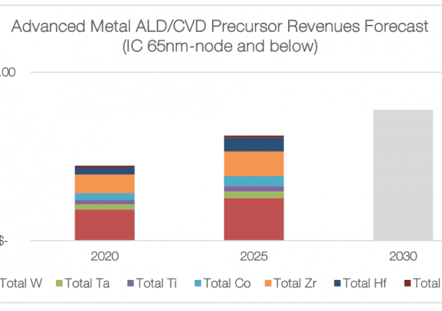
Global Market Remains Strong for ALD & CVD Precursors in IC Fabs
TECHCET—the advisory services firm providing electronic materials information— announced that the global market for atomic layer deposition (ALD) and chemical vapor deposition (CVD) precursors is showing strong growth despite semiconductor fabrication market challenges in 2019.
Plessey’s microLED Patented Growth Technology Combines Native Blue and Native Green Epitaxy on a Single Wafer
Plessey, an embedded technologies developer at the forefront of microLED technology for augmented and mixed reality (AR/MR) display applications has extended the capability of their proprietary GaN-on-Silicon process to enable Native Blue and Native Green emission from the same wafer.
Global Semiconductor Sales Down 15.9 Percent Year-to-Year in August
The Semiconductor Industry Association (SIA) today announced worldwide sales of semiconductors were $34.2 billion in August 2019, a decrease of 15.9 percent from the August 2018 total of $40.7 billion but 2.5 percent more than the July 2019 total of $33.4 billion. Monthly sales are compiled by the World Semiconductor Trade Statistics (WSTS) organization and represent a three-month moving average. SIA represents U.S. leadership in semiconductor manufacturing, design, and research.
Curved Nanochannels Allow Independent Tuning of Charge and Spin Currents
To increase the efficiency of microchips, 3D structures are now being investigated. However, spintronic components, which rely on electron spin rather than charge, are always flat. To investigate how to connect these to 3D electronics, University of Groningen physicist Dr. Kumar Sourav Das created curved spin transport channels. Together with his colleagues, he discovered that this new geometry makes it possible to independently tune charge and spin currents.
Spying on Topology
Topological insulators are quantum materials, which, due to their exotic electronic structure, on surfaces and edges conduct electric current like metal, while acting as an insulator in bulk. Scientists from the Max-Born Institute for Nonlinear Optics and Short Pulse Spectroscopy (MBI) have demonstrated for the first time how to tell apart topological materials from their regular – trivial – counterparts within a millionth of a billionth of a second by probing it with ultra-fast laser light.
New Version of Most Widely Used Camera and Imaging Interface—MIPI CSI-2—Designed to Build Capabilities for Greater Machine Awareness
The MIPI Alliance, an international organization that develops interface specifications for mobile and mobile-influenced industries, today announced major enhancements to MIPI Camera Serial Interface-2 (MIPI CSI-2), the most widely used camera specification in mobile and other markets.