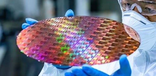
The lithography materials market is set for stronger growth in 2025 as semiconductor wafer starts rise and advanced device manufacturing gains traction. Over the next five years, TECHCET projects the total market to exceed $6.35B USD by 2029, at a 5.7% CAGR, fueled by rising wafer starts and added lithography layers at advanced nodes according to TECHCET’s 2025-2026 Critical Materials Report™ on Lithography.
- Revenues for all wafer fabrication lithography materials are forecasted to increase +6.0% to $5.1B USD
- A modest +2.2% recovery in 2024 ($4.81B USD)
- 2025 growth projections are as follows:
- Photoresists are projected to grow +4.9%
- Ancillaries +8.2%
- Extensions +6.7%
- EUV resists leading at +38% as adoption expands in logic and memory
Growth is being propelled by the increasing use of EUV lithography in high-volume manufacturing at Samsung, Intel, TSMC, SK Hynix and Micron, as logic transitions to gate-all-around nodes and DRAM incorporates 1 to 3 EUV layers. While High NA EUV development is progressing, cost-of-ownership hurdles remain, and new material platforms for EUV such as negative tone resists, metal oxide resists, dry-deposited resists, and directed self-assembly are under evaluation. Nanoimprint lithography is also making progress as a low cost-of-ownership alternative for KrF processes. Legacy platforms like I-Line, G-Line, and KrF continue to support mature devices. KrF is used for larger dimension features in advanced logic, NAND and DRAM nodes, although these are moving to ArF as dimensions shrink. Demand from AI-driven applications, particularly high-bandwidth memory and advanced logic, is also adding momentum to lithography volumes and revenues growth.
Looking ahead, the market will be increasingly shaped by advances in device architectures and integration schemes. Gate-all-around transistors, 3D NAND scaling, DRAM (and eventually 3D DRAM) and high-bandwidth memory demand are driving more process steps per wafer, tighter performance specifications and a need for controlled of cost-of-ownership. This is spurring new collaborations between material suppliers, equipment makers, and device manufacturers to refine resists and ancillaries for improved overlay precision, defect control, and line edge roughness. As lithography evolves in parallel with deposition (ALD/CVD/PVD) and etch processes, its role remains central in enabling next-generation semiconductor performance and production efficiency.
For more details on the Lithography market growth trajectory, including information on suppliers like JSR, TOK, Shin Etsu, Sumitomo, Dongjin, DuPont/Qnity, Fujifilm, EMD/Merck, Dongjin, Brewer Science, and more, go to: https://techcet.com/product/lithography-materials/