DEEPAK ANANDAN, Process Lead, Orbit & Skyline
Silicon is an abundant material on Earth, and its ability to form high-quality native oxide has made it dominant in low-power logic applications. Si plays a crucial role in low-power computation, digital and analog circuits, and memory devices. Additionally, Si power devices significantly impact power conversion, offering low cost but suffering from high power loss-key factors for customers seeking efficient solutions. Specifically, Si power MOSFETs and Si-IGBTs are well-suited for applications with switching frequencies below 10 kHz. Si-IGBTs are ideal for high-power applications above 3 kW, where magnetic components cannot be easily miniaturized with good-cost performance trade-off.
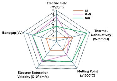
However, the footprint of Si is limited in high-efficiency power conversion applications for Electric Vehicles (EVs), Photovoltaics (PV), and other high-power potential applications due to its low critical electric field, threefold lower saturation velocity, and thermal conductivity compared to its competitors, such as SiC and GaN as shown in Fig.1. SiC and GaN, deliver exceptional performance in demanding applications such as inverters, battery charging systems, and DC-DC converters, offering minimal energy loss and enhanced heat dissipation. In contrast, Si typically requires expensive heat dissipation systems to manage thermal challenges in high-power applications.
Silicon single crystal growth is a well-matured process, enabling high-throughput production with a small seed crystal and a high growth rate at approximately 1450°C in a controlled furnace environment. It exhibits very low defect density and, as a low-bandgap material, offers excellent doping flexibility. Additionally, silicon is relatively easy to polish compared to harder materials like SiC (4H, 6H) and GaN, making it a preferred choice for large-scale semiconductor manufacturing.
SiC and GaN have high Mohs hardness, with values of 9 and 8.5, respectively. However, SiC presents significant challenges in growth due to its non-stoichiometric nature, making it difficult to grow like silicon. It requires extremely high temperatures, typically above 2200°C, and a high-quality, larger-size single crystal seed. Controlling polytypes is crucial in SiC growth, as it has more than 250 different polytypes. The typical sublimation method for 4H SiC boule growth produces approximately 50mm thick boules. Converting these boules into pucks and then wafers results in substantial material loss, leading to low throughput.
On the other hand, growing single GaN wafers is highly challenging due to the formation of highly defective crystal growth. Additionally, the smaller wafer size increases production costs. For commercial applications, the industry often opts for growing high-quality III-N layers on engineered foreign substrates such as SiC, Si, and sapphire, depending on the application. For power devices, substrates with good thermal conductivity, such as Si and SiC, are preferred due to their superior heat dissipation capabilities, whereas sapphire, with its poor thermal conductivity, is less suitable.
Key points: SiC and GaN, both wide bandgap materials, enable high blocking voltage with thin layers. However, the limited availability of large GaN substrates necessitates exploring foreign substrate integration. SiC wafer preparation remains costly due to its low sublimation rate and the challenges of processing this hard material, leading to significant OD and kerf losses.
Click here to read the full article in Semiconductor Digest.