Embracing and integrating new component-level technologies is a way to measurably improve quality, safety and yield.

A New Framework: Opportunities of Open Access for Optimizing Yield in Semiconductor Manufacturing
An open, secure monitoring and intelligence transaction platform would empower chip manufacturers to solve their problems and optimize their operations, their way.
An Interview with Kistler’s Robert Hillinger
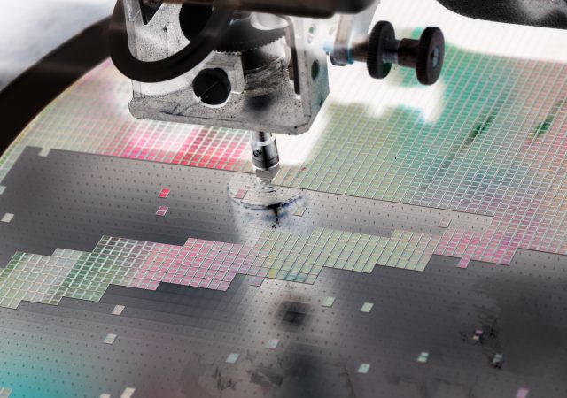
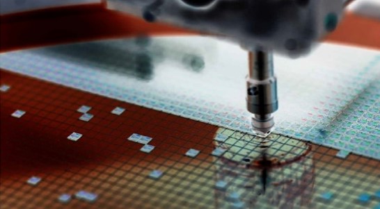
Robert Hillinger, Business Development Manager at Kistler, explains how dynamic force measurement increases process reliability in semiconductor production.
MEMS Mirrors for LIDAR
Clever integration of new microelectronic/nanoelectronic technologies will continue to provide increased functionalities for modern products. Light Imaging, Detection, And Ranging (LIDAR) technology uses lasers to see though fog and darkness, and smaller less expensive LIDAR systems are needed for autonomous…
Broadening Scope of SEMICON
Once upon a time, SEMICONs were essentially just for semiconductor manufacturing business and technology, and predominantly CMOS ICs. Back when we followed public roadmaps for technology to maintain the cadence of new manufacturing nodes in support of Moore’s Law, it…
Omhi kept us Ultra-Clean
Sadly, I just recently learned from the UCPSS 2016 website that Ohmi-sensei—Professor Doctor Tadahiro Ohmi—passed away in Sendai on 21 February 2016. As the guru of ultra-clean technology, he established the global Ultra Clean Society in 1988, founded the International…
Chasing IC Yield when Every Atom Counts
Increasing fab costs coming for inspection and metrology At SEMICON West this year in Thursday morning’s Yield Breakfast sponsored by Entegris, top executives from Qualcomm, GlobalFoundries, and Applied Materials discussed the challenges to achieving profitable fab yield for atomic-scale devices…