Cadence Design Systems, Inc. today announced that the Cadence digital full flow has achieved certification for the Samsung Foundry 5nm Low-Power Early (5LPE) process with Extreme Ultraviolet (EUV) lithography technology.
Jim Cable Tapped by Murata for Semiconductor Expansion Evaluation
pSemi Corporation today announced that its parent company, Murata, has selected chairman and chief technology officer Jim Cable to spearhead its semiconductor research and development (R&D) growth plans.
Samsung Accelerates New Product Ramp for 7nm Technology Node Using Synopsys’ Yield Explorer
Synopsys, Inc. announced successful deployment of Synopsys’ Yield Explorer yield learning platform for fast ramp-up of new products on Samsung’s advanced FinFET technology nodes.
‘Tsunami’ On a Silicon Chip: A World First For Light Waves
Sydney-Singapore team manipulates soliton photonic waves on a silicon chip.
Global Semiconductor Sales Decrease 14.6 Percent Year-to-Year in May
All regional markets down compared to last year, but global sales increase slightly on a month-to-month basis.

EV Group Revolutionizes Lithography With New Maskless Exposure Technology
EV Group (EVG) today unveiled MLE (Maskless Exposure), a revolutionary next-generation lithography technology developed to address future back-end lithography needs for advanced packaging, MEMS, biomedical and high-density printed circuit board (PCB) applications.
SEMI Smart Manufacturing Initiative Releases Groundbreaking Industry Benchmark Survey
The SEMI Smart Manufacturing Initiative today released the semiconductor industry’s first Benchmark Survey to assess the current implementation level of automation and control measures aimed at increasing productivity and efficiency in front-end semiconductor fabs.
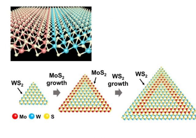
Atomic ‘Patchwork’ Using Heteroepitaxy For Next Generation Semiconductor Devices
Continuous process for engineering 2D transition metal dichalcogenide (TMDC) heterostructures.

SEMI Americas and Semiconductor Digest Announce 2019 “Best of West” Award Finalists: CyberOptics, Advantest and Edwards
SEMI and Semiconductor Digest today announced finalists for the Best of West award to be presented at SEMICON West 2019, July 9-11 at the Moscone Center in San Francisco.

Smart Parking and Sensors in the Age of IoT
Poorly managed parking resources have a substantial negative impact on cities — one that has been well-documented.