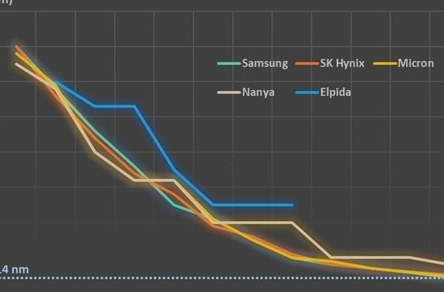
Innovation in memory technology is constant. In this article, TechInsights’ Jeongdong Choe reviews the latest developments in DRAM, NAND, and emerging technology, and provide insight on the trends in this space.
Editor’s Picks
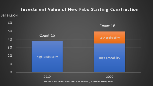
Fabs Valued at Nearly $50 Billion to Start Construction in 2020
Investments in new fab projects starting construction in 2020 is expected to reach nearly US$50 billion, up about US$12 billion from 2019, according to the latest update of the World Fab Forecast from SEMI.

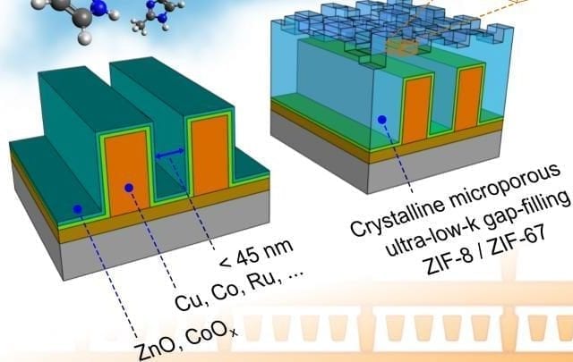
New Insulation Technique Paves The Way For More Powerful and Smaller Chips
Researchers at KU Leuven and imec have successfully developed a new technique to insulate microchips.
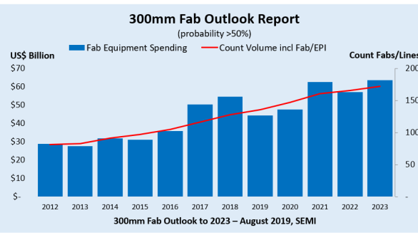
300mm Fab Equipment Spending to Seesaw, Reach New Highs in 2021 and 2023
300mm fab equipment spending will slowly recover in 2020 after the 2019 downturn and take off in 2021 to log a new record high topping US$60 billion, only to lag again in 2022 and rebound to an all-time peak in 2023, according to the SEMI Industry Research and Statistics group in its first edition of the 300mm Fab Outlook report.
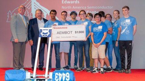
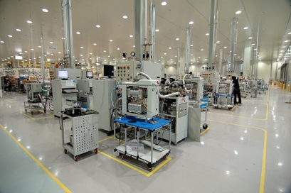
Edwards Celebrates Grand Opening of New ‘Green’ North America Semiconductor Technology Center in Hillsboro
Celebrating 100 years of innovation this year, Edwards opens new North America Semiconductor headquarters office on Century Boulevard.
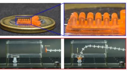
Researchers Develop Process Flow for High-Res 3D Printing of Mini Soft Robotic Actuators
SUTD, SUSTech and ZJU researchers’ proposed process flow guides 3D printing of miniature soft pneumatic actuators. Integrating the prints into a robotic system offers potential applications in jet-engine maintenance and minimally invasive surgery.

3D Optical Sensing Ready for Prime Time
The 3D optical sensing market is once again surging – and it’s all thanks to Apple. What will we see in the next wave of end products enhanced by this technology, how will other market segments approach – and eventually use – 3D optical sensing, and which suppliers stand to gain the most from this very vital technology?
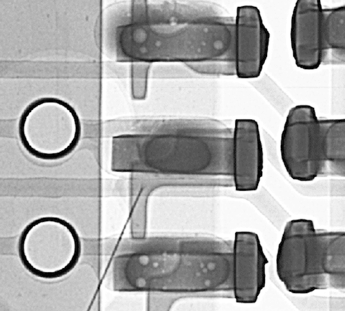
X-ray and Ultrasound Pinpoint Structural Defects in Microelectronic Components
Internal structural anomalies have nowhere to hide when
X-ray and ultrasound are used in combination.
100 Years of Vacuum Innovation – A Critical Enabler for Semiconductor Manufacturing
A look back at the history of vacuum technology and a look
forward into the future.