Increasing fab costs coming for inspection and metrology
Qualcomm – Geoffrey Yu
Double-patterning will be needed for metal and via layers as we go before 90nm pitch for the next generations of ICs. Qualcomm is committed to designing IC with smaller features, but not all companies may need to do so. Fab costs keep going up for atomic-scale devices…and there are tough trade-offs that must be made, including possibly relaxing reliability requirements. “Depending on the region. If you’re in an emerging region maybe the reliability requirements won’t be as high,” said Yu. Through-Silicon Vias (TSV) will eventually be used to stack IC layers, but they add cost and will only be used when performance cannot be met with cheaper solutions. “An early idea was to use TSV for logic:memory,” reminded Yu, “but then there was innovation to LPDDR4 allowing it deliver the same bandwidth with one-half the power of LPDDR3, which delayed TSV.”
GlobalFoundries – Harry Levenson
“A more expensive part could provide a better value proposition for a customer,” reminded Levenson as he discussed the challenges of inspecting next-generation commercial ICs in high-volume manufacturing (HVM). “We still have clear demand for products to run in HVM at the leading edge, but we are now in the world of double-patterning and this applies to optical inspection as well as imaging.” Requirements for inspection and imaging are different, but he same physics applies. In imaging Depth of Focus (DoF) of ~140nm is generally preferred, while the same used for inspection of a <140nm thin film would to induce noise from lower-levels. We can’t do e-beam inspections due to too much energy concentration needed to get acceptable throughput (and the challenge gets worse as the pixel area is reduced, inherently slowing down throughput). However, e-beams are helpful because they can detect open contracts/vias in metal levels due to the conductivity of electrons providing additional contrast compared to any possible optical inspection.
Applied Materials – Sanjiv Mittal
Mittal discussed how the CMOS transistor gate formation process has increased in complexity over the last few device generations: 8x more unit-process steps, 3x higher fab cost, 50x lower defects needed for yield. “The challenges are immense,” admitted Mittal. “What happens when you try to work on yield improvement when you’re ramping volume? At the same time you’re trying to improve yield by making changes, you’re trying to increase the volume by not making changes.”
Entegris – Jim O’Neill
O’Neill is CTO of the combined Entegris post-merger with ATMI, and was recently director of advanced process R&D for IBM. Since Entegris provides materials and sub-systems, in the simplest cases the company works to improve IC fab yield by minimizing defects. “However, the role of the materials-supplier should change,” averred O’Neill. “The industry needs bottle-to-nozzle wet chemistry solutions, and applications-based clean gas delivery.” In an exclusive interview with SST/SemiMD, O’Neill provided as example of a ‘wetted process solution’ a post-CMP-clean optimized through tuning of the brush polymer composition with the cleaning chemistry.
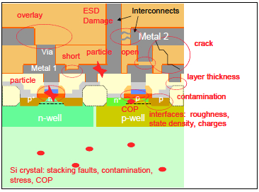
ITRS Difficult Challenges for Yield 2013-2020
- Existing techniques trade-off throughput for sensitivity, but at expected defect levels, both throughput and sensitivity are necessary for statistical validity.
- Reduction of inspection costs and increase of throughput is crucial in view of CoO.
- Detection of line roughness due to process variation.
- Electrical and physical failure analysis for killer defects at high capture rate, high throughput and high precision.
- Reduction of background noise from detection units and samples to improve the sensitivity of systems.
- Improvement of signal to noise ratio to delineate defect from process variation.
- Where does process variation stop and defect start?
—E.K.