
Jeongdong Choe, PhD., TechInsights, Ottawa, Canada
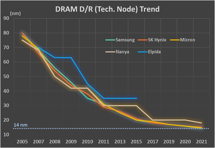
DRAM cell scaling down to a 17nm design rule has already been productized by major DRAM players including Samsung, Micron and SK Hynix (Figure 1). Currently, they are developing n+1 (16nm) and n+2 (15nm or beyond) so-called 1z, 1a and 1b generation devices, which means the DRAM cell design rule might be able to further scale down to sub-15 nm without adopting Extreme Ultraviolet (EUV) lithography for DRAM cell patterning.
The cell design scaling down process is slowing due to many scaling issues including patterning, leakage and sensing margin. And so far, EUV adoption on DRAM process is not cost effective. It appears that the 14nm DRAM cell design rule would be the last node if DRAM cell architecture keeps the current 1T1C with B-RCAT and cylindrical capacitor.

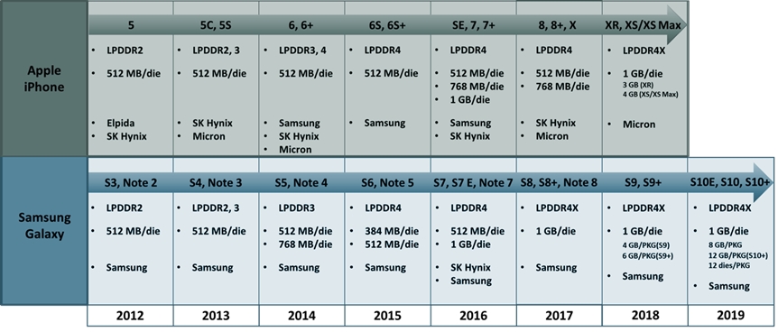
An examination of teardowns and analyses of recently released smartphones found that the phones use 1x nm and 1y nm design rule LPDDR4X DRAM devices (Figure 2). For example, Samsung’s Galaxy S10 products like the S10, S10+ and S10 5G have 1y nm LPDDR4X devices with an 8 Gb DRAM die floor plan in the 8 GB or 12 GB package. These devices contain 8 or 12 dies in the package.

Bit density on DRAM die reached 0.237 Gb/mm2 on Samsung’s 1y nm LPDDR4X 8 Gb die, which is a 25.4% increase from the 1x LPDDR4X die (Figure 3). Micron recently introduced its 1y nm 8 Gb DDR4 DRAM die with 0.205 Gb/mm2, a 22.7% increase from its 1x DDR4 die. Additionally, SK Hynix 1x LPDDR4 technology uses a 0.191 Gb/mm2 bit density.

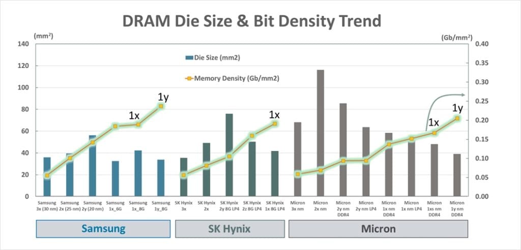
Figure 4 shows a comparison of DRAM cell size from three major players, including the Samsung 1y nm and Micron 1y nm technology nodes. It is clear that Micron’s 1x nm cell size was the same as Samsung’s 2y nm, while Micron’s 1y nm cell size (0.0024 µm2) is very close to Samsung’s 1y nm (0.0023 µm2).

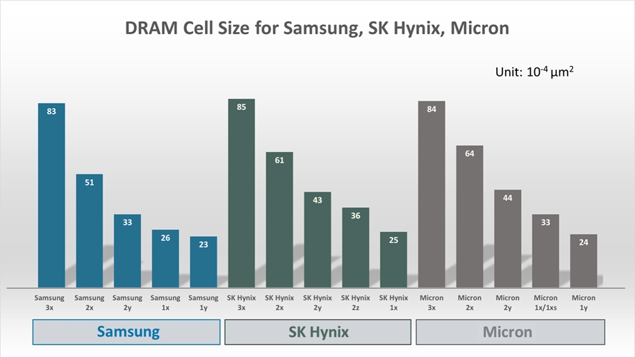
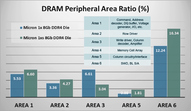
Micron changed its cell design from the 1x nm technology node and kept it on 1y. They also revealed a 1xs version, which is a die shrink version of 1x nm on a DDR4 8 Gb die. Micron uses the same design rule on DRAM cell array, while optimizing the memory peripheral design, especially on the write driver and column decoder/amplifier circuitry. Figure 5 shows a comparison of the Micron 1x and 1xs DDR4 DRAM dies from a peripheral functional block area ratio view.

SK Hynix’ cell capacitor design and process have changed from cylindrical capacitor to pillar. Although their 1x nm DRAM cell capacitor structure has the same process as their previous cylindrical capacitor, they insert a-Si into the inner capacitor, which means they only use the outer surface.
When it comes to graphic DRAM (GDRAM), both Samsung and Micron Technology revealed 8 Gb GDDR6 packages with 8 Gb GDRAM dies for the NVIDIA GeForce RTXTM 2080. Samsung uses a 1x nm design rule with 0.303 Gb/mm2 bit density, while Micron Technology uses 2y nm design rule with 0.093 Gb/mm2 bit density. Samsung also introduced the world’s first 16 Gb 1x nm GDRAM die for GDDR6 applications such as NVIDIA QuadroRTXTM 5000. Its bit density is 0.332 Gb/mm2, which is the highest on a DRAM to date.
For high bandwidth memory applications, SK Hynix, Samsung, and Intel have commercially available HBM2 devices; only Micron has an HMC2 available. SK Hynix HBM2 products used on AMD Vega 10XT have a 2z nm tech node. The Samsung NVIDIA Tesla P100PCIe and Intel SR3RM eighth generation Quad CoreTM i5-8305G HBM2 products use Samsung’s 2y nm HBM2 dies. Micron keeps the old DRAM cell design (3x nm) for HMC2 DRAM dies stacked together with an IBM 1234A controller die in the package.
NAND technology
All the major NAND die manufacturers have introduced 9XL 3D NAND devices. Samsung 92L V-NAND (V5), Toshiba and Western Digital Company (Western Digital) 96L BiCS4, Intel/Micron 96L FG CuA are already on the market, while the SK Hynix 96L PUC is expected to be released this year.
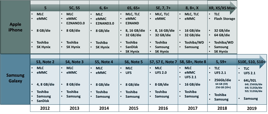
There have been many changes made when compared to the previous 3D NAND 64L and 72L generation. Samsung’s single vertical channel hole (VCH) etching technology is unique and may be used on their next generation (128L) as well. Samsung introduced both 256 Gb die and 512 Gb die with their 92L V-NAND technology. Toshiba/Western Digital changed NAND string architecture from single stack (64L) to double stack (48L+48L), which is different from Samsung’s 92L. They also adopted a two-step metal contact etching process. Until 2016, all smartphones used 2D NAND; since 2017, both 2D and 3D NAND devices have been used on smartphones. Today’s Samsung Galaxy and Apple iPhone, for example, utilize only 3D NAND devices as shown in Figure 6.

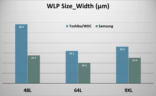
The word line pad (WLP) connection area, the so-called staircase region, can be increased due to the number of total gates increased. All 3D NAND manufacturers newly optimized and designed the trim masks and process integration to reduce the area and cost/throughput. For example, Figure 7 shows a comparison of WLP connection area from Samsung and Toshiba/Western Digital on 48L, 64L and 92L/96L. The WLP connection area is just 0.82% of the full 64L die, and increased only by 13%, from 64L to 96L for Toshiba/Western Digital. Samsung has more effectively designed the trim (or slim) masks so that the penalty region is smaller than Toshiba/Western Digital’s, generation after generation.

Samsung, Toshiba and Western Digital still use a selective epitaxial grown Si (SEG) process for the ground selector, which means they use the same source erase method as 64L products. Intel and Micron again stacked two NAND strings such as 48L plus 48L on CMOS circuitry called CMOS under Array (CuA). They keep the FG instead of using a CTF layer for the storage. SK Hynix 96L V4 periphery under cell (PUC) structure, or 4D NAND, is quite different from their previous P-BiCS. They removed pipe control gates, and for 9XL 3D NAND cell integration, they use their own unique vertical channel capping structures.
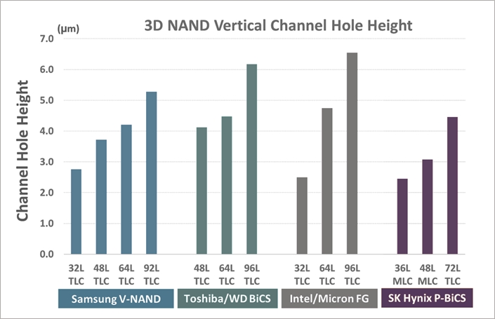
As the total number of gates increases, the vertical channel hole (VCH) height increases as shown in Figure. 8. Toshiba/Western Digital 96L and Intel/Micron 96L VCH’s is over 6 µm. Both use double stacked 96L (two-step VCH etching). For the interface between two stacks, Intel and Micron Technology use multi-layer dielectrics (64L) or SiN layer only (96L), while Toshiba and Western Digital use SiO layer only.

Today, 512 Gb 3D NAND dies are common. For example, Samsung offers both 512 Gb 64L TLC and 512 Gb 92L TLC dies. SK Hynix provides a 512 Gb 72L TLC die and Intel/Micron sells a 512 Gb 96L die.
3D NAND QLC devices are also available, especially from Samsung, Intel and Micron with 1 Tb 3D NAND die. Their bit densities are 5.6 Gb/mm2 (for Samsung 64L QLC die) and 6.5 Gb/mm2 (for Intel 64L QLC die), respectively. Intel/Micron keep a tile-type floor plan on their 64L QLC die and 96L TLC die.
Samsung also revealed its Z-NAND (Z-SSD) for the fast NAND application which may be competitive with Intel XPoint or Toshiba XL-FLASH. The first generation of Samsung’s Z-NAND SSD products use 48L V-NAND cell array on 64 Gb SLC Z-NAND dies stacked together with one F-chip die in a package.
Embedded and emerging memory technology
As demand for embedded memories and MCU applications for AI and IoT increases, emerging memory technologies are also on the rise. In addition, Intel has been applying their XPoint memory devices into NAND and storage products such as Optane SSD, Optane DC SSD, DC PM and even NVDIMM application. Emerging memories consist of MRAM, including STT-MRAM and SOT-MRAM, PCRAM including XPoint, ReRAM including CBRAM, OxRAM and Memristor, FeRAM and others including NRAM.
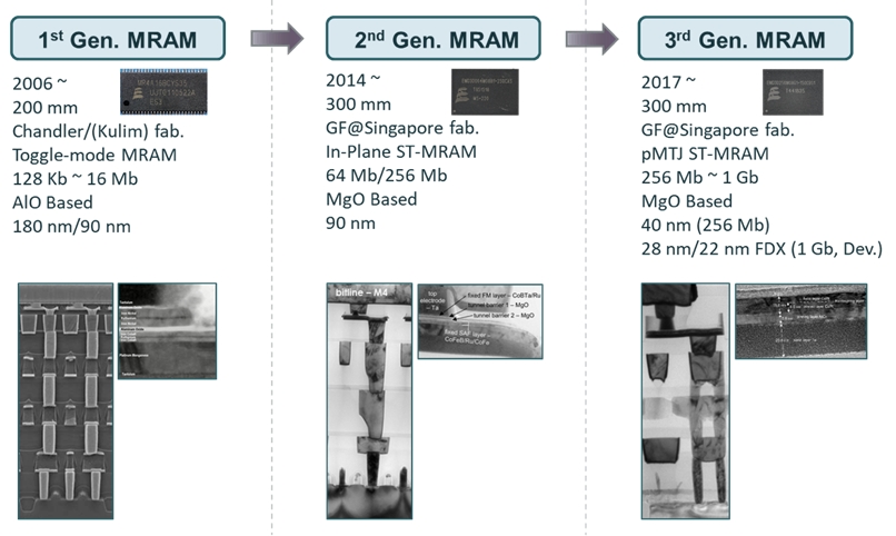
Everspin Technology already released its 256 Mb pMTJ STT-MRAM products. Everspin’s first generation MRAM was a toggle-mode and AlO-based 180nm/90 nm product. Now, they market 64 Mb/256 Mb in-plane MTJ 90nm STT-MRAM and 256 Mb pMTJ 40 nm STT-MRAM products. Working together with Global Foundries, their 28nm/22nm FDX 1 Gb STT-MRAM is expected to be available soon. Figure 9 shows Everspin Technologies’ MRAM products review.

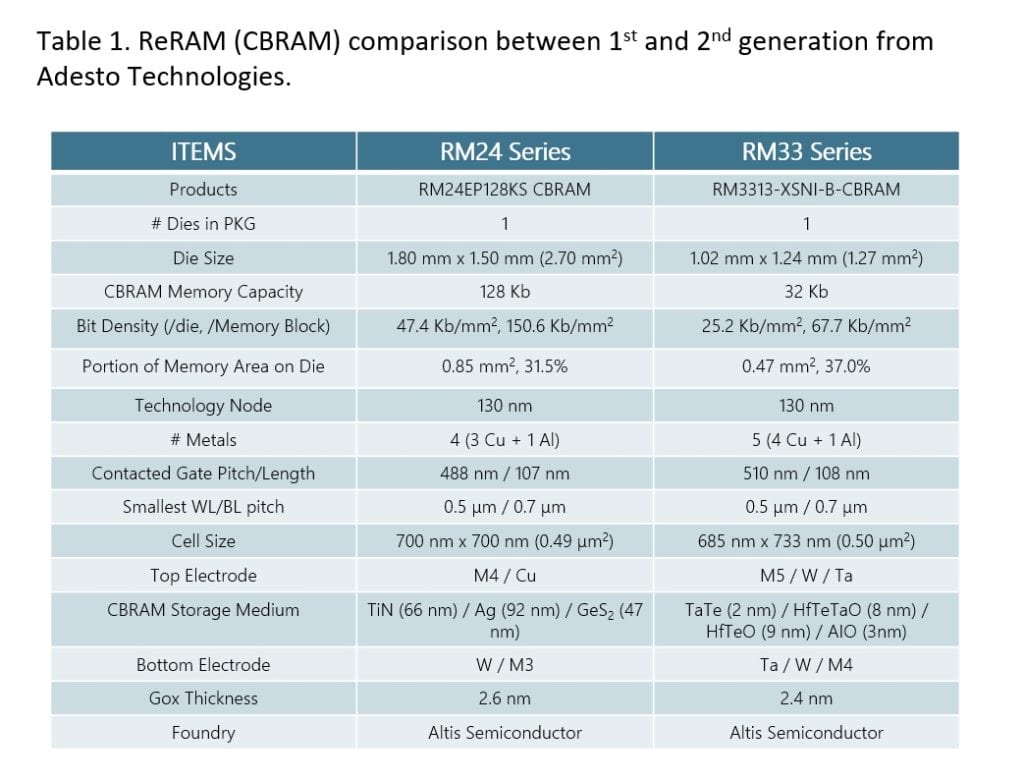
Adesto Technology produced its second generation CBRAM, and is working on its third-generation solutions. The second generation used the same cell design rule as the first generation. However, the number of metals and CBRAM storage medium materials changed completely from Ag/GeS to Hf- and Te-based to a multi-layered structure. Many major DRAM, NAND and logic makers are eager to jump into emerging memory markets. We anticipate seeing new memory products throughout 2019 and into 2020, including Samsung’s 28 nm FDSOI STT-MRAM, TSMC eSTT-MRAM and eReRAM, Intel 22FFL STT-MRAM, Micron XPoint QunantX and Panasonic/UMC 28nm FDX ePCM. Table 1 briefly describes a comparison of ReRAM (CBRAM) first and second generation from Adesto Technologies.

Conclusion
TechInsights continually monitors innovations in DRAM, NAND and emerging technology products. Roadmaps detailing our findings and insights are available through TechInsights’ website and are regularly updated. TechInsights memory analysis is available through subscription products or individual reports. For more information, visit the TechInsights website.
About the author
Dr. Jeongdong Choe is a Senior Technical Fellow at TechInsights. He holds a Ph.D. in electronic engineering and has over 27 years’ experience in semiconductor process integration for DRAM, (V)NAND, SRAM and logic devices. Dr. Choe’s background includes positions as a Team Lead in R&D for SK-Hynix and Samsung, where he optimized process and device architectures with state-of-the-art technologies for mass production.