A new metrology system uses spectroscopic ellipsometry at mid-infrared wavelengths to provide accurate critical dimension and profile measurements of high-aspect-ratio (HAR) holes in 3D NAND memory. This information is essential for developing and controlling the fabrication process. The non-destructive technique exploits unique optical properties of mid-IR radiation to extract information that has not previously been available on a robust platform suitable for in-fab use.
In the cover story of the March issue of Semiconductor Digest, authors from Onto Innovation and Micron Technology look at two examples: channel holes, which have aspect ratios as high as 60:1 and eventually become vertical strings of memory cells in 3d NAND memory, and the holes in the hardmask, which have aspect ratios up to 25:1 and are used to etch the channel holes.

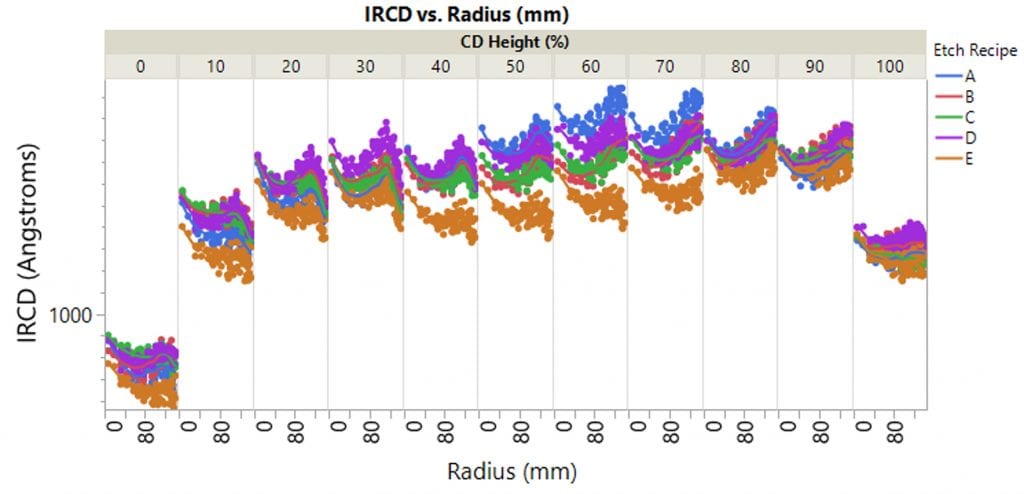
The feature explores how IRCD addresses the shortcomings of conventional ultraviolet to near-infrared OCD in channel hole etch high-fidelity z-profile and amorphous carbon hardmask etch BCD metrology. The novel IRCD technology and modeling enable HAR 3D NAND etch process monitoring and feedback in both the development and high-volume manufacturing phases for current and next generation 3D-NAND structures. We expect to discover other IRCD applications as we continue to explore the physics of light interaction with relevant materials and structures, particularly when observed mid-IR optical phenomena differ from those seen at traditional OCD wavelength ranges.