YULEI SUN, SHELBY CRAIN and STEVE MCWILLIAMS, Onto Innovation
Over the past 10 years, primarily driven by a tremendous expansion in the availability of data and computing power, artificial intelligence (AI) and machine-learning (ML) technologies have found their way into many different areas and have changed our way of life and our ability to solve problems. Today, artificial intelligence and machine learning are being used to refine online search results, facilitate online shopping, customize advertising, tailor online news feeds and guide self-driving cars. The future that so many have dreamed of is just over the horizon, if not happening right now.
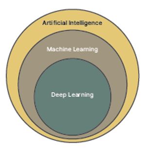
The term artificial intelligence was first introduced in the 1950s and used famously by Alan Turing. The noted mathematician and the creator of the so-called Turing Test believed that one day machines would be able to imitate human beings by doing intelligent things, whether those intelligent things meant playing chess or having a conversation. Machine learning is a subset of AI. Machine learning allows for the automation of learning based on an evaluation of past results against specified criteria. Deep learning (DL) is a subset of machine learning (FIGURE 1). With deep learning, a multi-layered learning hierarchy in which the output of each layer serves as the input for the next layer. A recurrent neural network is an example of this.

Currently, the semiconductor manufacturing industry uses artificial intelligence and machine learning to take data and autonomously learn from that data. With the additional data, AI and ML can be used to quickly discover patterns and determine correlations in various applications, most notably those applications involving metrology and inspection, whether in the front-end of the manufacturing process or in the back-end. These applications may include AI-based spatial pattern recognition (SPR) systems for inline wafer monitoring [2], automatic defect classification (ADC) systems with machine-learning models and machine learning-based optical critical dimension (OCD) metrology systems [1][7].
However, AI and ML face significant challenges when confronted with new and previously uncharacterized situations. In other words, they don’t have enough previous data to discover those patterns and determine those correlations.
By combining AI and ML techniques with more traditional approaches — like physical modeling — the performance of metrology and inspection systems can be significantly improved, allowing such systems to better adapt to previously unfamiliar data or uncharacterized situations. One such example, a synergized physical modeling and machine-learning-hybrid approach has shown to better predict OCD results.
While all of this seems quite straightforward — using constant streams of data to solve problems — it is not that simple to build and deploy a deep-learning model, especially in a high-mix manufacturing environment. In that scenario, the help of the human hand – in other words, human expertise – is needed to sort through the data to separate meaningful data from not-so-meaningful data.