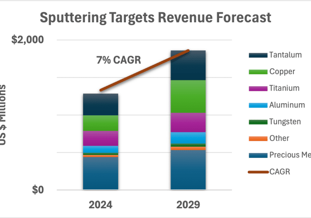
TECHCET projects semiconductor sputtering target revenues to grow near 9% in 2025, reaching $1.45 billion.
Packaging
European Chips Skills Academy Launches ECS Summer School 2025 to Inspire Future Electronics Talent
The European Chips Skills Academy (ECSA), an EU-funded project coordinated by SEMI Europe, in collaboration with industry partners AENEAS, EPoSS, and INSIDE, has announced the launch of the ECS Summer School 2025.
FormFactor Doubles Capacity at Taiwan Service Center to Meet Growing Demand
Strategic investment enhances local capabilities to elevate customer support and satisfaction with FormFactor products.
Ansys Semiconductor Solutions Certified by TSMC for Reliable, Accurate Analysis of Evolving Chip Designs
Ansys today announced that PathFinder-SC is certified as a new ESD analysis solution for customers designing with TSMC’s N2 silicon process technology.
Sivers Semiconductors Announces Strategic OEM Partnership with O-Net Technologies
Sivers Semiconductors AB today announced a strategic partnership with O-Net Technologies to produce high-performance external laser sources, a critical component enabling next-generation AI data center architectures.
Altera Starts Production Shipments of Industry’s Highest Memory Bandwidth FPGA
Altera Corporation today announced production shipments of its Agilex 7 FPGA M-Series, the industry’s first high-end, high-density FPGA to feature integrated high bandwidth memory and support for DDR5 and LPDDR5 memory technologies
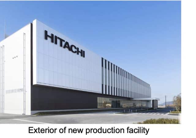
Completion of New Production Facility for Semiconductor Manufacturing Equipment in Kasado Area
Hitachi High-Tech Corporation announced that the new production facility for semiconductor manufacturing equipment was completed and started the operation on March 17, 2025.
NEDO Approves Rapidus’ FY2025 Plan and Budget for 2nm Semiconductor Projects
Rapidus Corporation today announced that its plans and budget for fiscal year 2025 have been approved by Japan’s New Energy and Industrial Technology Development Organization (NEDO).
Teradyne Announces Production System for Double-Sided Wafer Probe Test for Silicon Photonics
This system is designed to meet the growing demand for high-throughput electro-optical testing of silicon photonic wafers driven by co-packaged optics (CPO) applications.
HieFo Introduces High Efficiency CW Lasers for Silicon Photonics Transceivers
HieFo announced today the product launch of multiple new high-efficiency Continuous Wave DFB indium phosphide (InP) lasers, designed to address the ever-increasing demands of silicon photonics based optical transceivers.